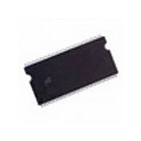
MT46V16M16P-5B:K Micron Technology Inc, MT46V16M16P-5B:K Datasheet - Page 62

MT46V16M16P-5B:K
Manufacturer Part Number
MT46V16M16P-5B:K
Description
DRAM Chip DDR SDRAM 256M-Bit 16Mx16 2.6V 66-Pin TSOP Tray
Manufacturer
Micron Technology Inc
Type
DDR SDRAMr
Datasheet
1.MT46V16M16P-5BK.pdf
(93 pages)
Specifications of MT46V16M16P-5B:K
Density
256 Mb
Maximum Clock Rate
400 MHz
Package
66TSOP
Address Bus Width
15 Bit
Operating Supply Voltage
2.6 V
Maximum Random Access Time
0.7 ns
Operating Temperature
0 to 70 °C
Organization
16Mx16
Address Bus
15b
Access Time (max)
700ps
Operating Supply Voltage (typ)
2.6V
Package Type
TSOP
Operating Temp Range
0C to 70C
Operating Supply Voltage (max)
2.7V
Operating Supply Voltage (min)
2.5V
Supply Current
260mA
Pin Count
66
Mounting
Surface Mount
Operating Temperature Classification
Commercial
Lead Free Status / RoHS Status
Compliant
Available stocks
Company
Part Number
Manufacturer
Quantity
Price
Company:
Part Number:
MT46V16M16P-5B:K
Manufacturer:
MICRON
Quantity:
6 589
Company:
Part Number:
MT46V16M16P-5B:K
Manufacturer:
MICRON
Quantity:
20 000
Company:
Part Number:
MT46V16M16P-5B:K
Manufacturer:
MICRON
Quantity:
7 580
Figure 26:
READ
PDF: 09005aef80768abb/Source: 09005aef82a95a3a
DDR_x4x8x16_Core2.fm - 256Mb DDR: Rev. O, Core DDR: Rev. B 1/09 EN
Command
BA0, BA1
Address
CK#
CK
Example: Meeting
Bank x
Row
ACT
T0
Note:
During the READ command, the value on input A10 determines whether or not auto
precharge is used. If auto precharge is selected, the row being accessed will be
precharged at the end of the READ burst; if auto precharge is not selected, the row will
remain open for subsequent accesses.
During READ bursts, the valid data-out element from the starting column address will
be available following the CL after the READ command. Each subsequent data-out
element will be valid nominally at the next positive or negative clock edge (that is, at the
next crossing of CK and CK#). Figure 27 on page 62 shows the general timing for each
possible CL setting. DQS is driven by the DDR SDRAM along with output data. The
initial LOW state on DQS is known as the read preamble; the LOW state coincident with
the last data-out element is known as the read postamble.
Upon completion of a burst, assuming no other commands have been initiated, the DQ
will go High-Z. Detailed explanations of
window hold), and the valid data window are depicted in Figure 35 on page 70 and
Figure 36 on page 71. Detailed explanations of
t
Data from any READ burst may be concatenated or truncated with data from a subse-
quent READ command. In either case, a continuous flow of data can be maintained. The
first data element from the new burst follows either the last element of a completed
burst or the last desired data element of a longer burst which is being truncated. The
new READ command should be issued x cycles after the first READ command, where x
equals the number of desired data element pairs (pairs are required by the 2n-prefetch
architecture). This is shown in Figure 28 on page 63. A READ command can be initiated
on any clock cycle following a previous READ command. Nonconsecutive read data is
illustrated in Figure 29 on page 64. Full-speed random read accesses within a page (or
pages) can be performed, as shown in Figure 30 on page 65.
AC (data-out transition skew to CK) are depicted in Figure 37 on page 72.
NOP
For the READ commands used in the following illustrations, auto precharge is dis-
abled.
T1
t RRD
t
RCD (
NOP
t
RRD) MIN When 2 <
T2
Bank y
ACT
Row
60
T3
t
Micron Technology, Inc., reserves the right to change products or specifications without notice.
RCD (
t
DQSQ (valid data-out skew),
NOP
T4
t
RRD) MIN/
t
DQSCK (DQS transition skew to CK) and
256Mb: x4, x8, x16 DDR SDRAM
t RCD
NOP
T5
t
CK ≤ 3
©2003 Micron Technology, Inc. All rights reserved.
RD/WR
Bank y
T6
Col
t
QH (data-out
Operations
Don’t Care
NOP
T7


