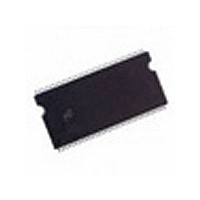
MT46V16M16P-5B:K Micron Technology Inc, MT46V16M16P-5B:K Datasheet - Page 56

MT46V16M16P-5B:K
Manufacturer Part Number
MT46V16M16P-5B:K
Description
DRAM Chip DDR SDRAM 256M-Bit 16Mx16 2.6V 66-Pin TSOP Tray
Manufacturer
Micron Technology Inc
Type
DDR SDRAMr
Datasheet
1.MT46V16M16P-5BK.pdf
(93 pages)
Specifications of MT46V16M16P-5B:K
Density
256 Mb
Maximum Clock Rate
400 MHz
Package
66TSOP
Address Bus Width
15 Bit
Operating Supply Voltage
2.6 V
Maximum Random Access Time
0.7 ns
Operating Temperature
0 to 70 °C
Organization
16Mx16
Address Bus
15b
Access Time (max)
700ps
Operating Supply Voltage (typ)
2.6V
Package Type
TSOP
Operating Temp Range
0C to 70C
Operating Supply Voltage (max)
2.7V
Operating Supply Voltage (min)
2.5V
Supply Current
260mA
Pin Count
66
Mounting
Surface Mount
Operating Temperature Classification
Commercial
Lead Free Status / RoHS Status
Compliant
Available stocks
Company
Part Number
Manufacturer
Quantity
Price
Company:
Part Number:
MT46V16M16P-5B:K
Manufacturer:
MICRON
Quantity:
6 589
Company:
Part Number:
MT46V16M16P-5B:K
Manufacturer:
MICRON
Quantity:
20 000
Company:
Part Number:
MT46V16M16P-5B:K
Manufacturer:
MICRON
Quantity:
7 580
Figure 22:
PDF: 09005aef80768abb/Source: 09005aef82a95a3a
DDR_x4x8x16_Core2.fm - 256Mb DDR: Rev. O, Core DDR: Rev. B 1/09 EN
Command
BA0, BA1
Address
V
V
DQS
DD
V
CK#
CKE
A10
V
DM
DQ
CK
TT
REF
DD
Q
1
t VTD 1
INITIALIZATION Timing Diagram
Notes:
LVCMOS
LOW level
Power-up: V
T = 200µs
1. V
2. Although not required by the Micron device, JEDEC specifies issuing another LMR command
3. The two AUTO REFRESH commands at Td0 and Te0 may be applied following the LMR com-
4.
5. While programming the operating parameters, reset the DLL with A8 = 1.
(
(
(
(
(
(
(
)
(
)
)
)
)
)
(
(
(
(
(
(
)
(
(
(
(
(
)
)
)
)
)
)
)
)
)
)
)
)
(
(
(
(
(
(
(
(
(
(
)
(
(
)
(
)
(
)
(
)
(
)
(
(
(
)
)
)
)
)
)
)
)
)
)
)
)
)
V
even if V
the V
specified range.
(A8 = 0) prior to activating any bank. If another LMR command is issued, the same, previ-
ously issued operating parameters must be used.
mand at Ta0.
t
DESELECTs are allowed), and 200 cycles of CK are required before a READ command can be
issued.
MRD is required before any command can be applied (during MRD time only NOPs or
DD
TT
TT
t IS t IH
t IS
and CK stable
NOP
, and V
T0
is not applied directly to the device; however,
High-Z
High-Z
TT
t IH
t CH
t CK
supply and the input pin. Once initialized, V
DD
REF
/V
t CL
All banks
DD
t IS t IH
≤ V
PRE
T1
Q are 0V, provided a minimum of 42Ω of series resistance is used between
DD
+ 0.3V. Alternatively, V
t RP
(
(
(
(
(
(
(
(
(
(
)
(
)
(
)
(
)
(
)
(
)
(
)
)
)
)
)
)
)
)
)
)
(
(
(
(
(
(
(
(
(
(
)
(
)
(
)
(
)
(
)
(
)
(
)
)
)
Load extended
)
)
)
)
)
)
)
mode register
t IS t IH
t IS t IH
t IS t IH
BA0 = 1
BA1 = 0
Code
Code
LMR
Ta0
54
t MRD
(
(
(
(
(
(
(
(
(
)
)
(
)
(
)
(
)
(
)
(
)
(
)
(
)
)
)
)
)
)
)
)
(
(
(
(
(
(
(
(
(
)
)
(
)
(
)
(
)
(
)
(
)
(
)
(
)
)
)
)
)
)
)
)
Load mode
register5
Code 3
BA0 = 0
BA1 = 0
Code
LMR
Tb0
Micron Technology, Inc., reserves the right to change products or specifications without notice.
t MRD
(
(
(
(
(
(
(
TT
)
)
)
)
)
)
)
(
(
(
(
(
(
(
(
(
)
)
)
)
)
)
)
)
)
(
(
(
(
(
(
(
(
)
(
)
(
)
(
)
(
)
(
)
(
)
(
(
)
)
)
)
)
)
)
)
)
may be 1.35V maximum during power-up,
All banks
t IS t IH
PRE
256Mb: x4, x8, x16 DDR SDRAM
Tc0
t
VTD ≥ 0 to avoid device latch-up. V
REF
t RP
(
(
(
(
(
(
(
(
)
(
)
(
)
(
)
(
)
(
)
(
)
(
(
)
)
)
)
)
)
)
)
)
(
(
(
(
(
(
(
(
(
(
)
(
)
(
)
(
)
(
)
(
)
(
)
)
)
)
)
)
)
)
)
)
must always be powered within the
200 cycles of CK4
Td0
AR
Indicates A Break in
Time Scale
©2003 Micron Technology, Inc. All rights reserved.
t RFC
(
(
(
(
(
(
(
(
(
(
)
(
)
(
)
(
)
(
)
(
)
(
)
)
)
)
)
)
)
)
)
)
(
(
(
(
(
(
(
(
)
(
)
(
)
(
)
(
)
(
)
(
)
(
(
)
)
)
)
)
)
)
)
)
Te0
AR
t RFC
(
(
(
(
(
(
(
Operations
(
)
(
)
(
)
(
)
(
)
(
)
(
)
(
(
)
)
)
)
)
)
)
)
)
(
(
(
(
(
(
(
(
)
(
)
(
)
(
)
(
)
(
)
(
)
(
(
)
)
)
)
)
)
)
)
)
ACT 2
Don’t Care
Tf0
BA
RA
RA
DD
Q,


