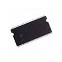
MT46V16M16P-5B:K Micron Technology Inc, MT46V16M16P-5B:K Datasheet - Page 42

MT46V16M16P-5B:K
Manufacturer Part Number
MT46V16M16P-5B:K
Description
DRAM Chip DDR SDRAM 256M-Bit 16Mx16 2.6V 66-Pin TSOP Tray
Manufacturer
Micron Technology Inc
Type
DDR SDRAMr
Datasheet
1.MT46V16M16P-5BK.pdf
(93 pages)
Specifications of MT46V16M16P-5B:K
Density
256 Mb
Maximum Clock Rate
400 MHz
Package
66TSOP
Address Bus Width
15 Bit
Operating Supply Voltage
2.6 V
Maximum Random Access Time
0.7 ns
Operating Temperature
0 to 70 °C
Organization
16Mx16
Address Bus
15b
Access Time (max)
700ps
Operating Supply Voltage (typ)
2.6V
Package Type
TSOP
Operating Temp Range
0C to 70C
Operating Supply Voltage (max)
2.7V
Operating Supply Voltage (min)
2.5V
Supply Current
260mA
Pin Count
66
Mounting
Surface Mount
Operating Temperature Classification
Commercial
Lead Free Status / RoHS Status
Compliant
Available stocks
Company
Part Number
Manufacturer
Quantity
Price
Company:
Part Number:
MT46V16M16P-5B:K
Manufacturer:
MICRON
Quantity:
6 589
Company:
Part Number:
MT46V16M16P-5B:K
Manufacturer:
MICRON
Quantity:
20 000
Company:
Part Number:
MT46V16M16P-5B:K
Manufacturer:
MICRON
Quantity:
7 580
PDF: 09005aef80768abb/Source: 09005aef82a95a3a
DDR_x4x8x16_Core2.fm - 256Mb DDR: Rev. O, Core DDR: Rev. B 1/09 EN
44.
45. During initialization, V
46. The current Micron part operates below 83 MHz (slowest specified JEDEC operating
47. When an input signal is HIGH or LOW, it is defined as a steady state logic HIGH or
48. Random address is changing; 50% of data is changing at every transfer.
49. Random address is changing; 100% of data is changing at every transfer.
50. CKE must be active (HIGH) during the entire time a REFRESH command is executed.
51. I
52. Whenever the operating frequency is altered, not including jitter, the DLL is required
53. This is the DC voltage supplied at the DRAM and is inclusive of all noise up to 20 MHz.
54. The -6/-6T speed grades will operate with
t
but specify when the device output is no longer driving (
(
Alternatively, V
provided a minimum of 42Ω of series resistance is used between the V
the input pin.
frequency). As such, future die may not reflect this option.
LOW.
That is, from the time the AUTO REFRESH command is registered, CKE must be
active at each rising clock edge, until
I
remain stable. Although I
to be reset followed by 200 clock cycles before any READ command.
Any noise above 20 MHz at the DRAM generated from any source other than that of
the DRAM itself may not exceed the DC voltage range of 2.6V ±100mV.
t
RPST end point and
DD
DD
RAS (MAX) = 120,000ns at any slower frequency.
t
RPRE).
2N specifies the DQ, DQS, and DM to be driven to a valid HIGH or LOW logic level.
2Q is similar to I
TT
may be 1.35V maximum during power-up, even if V
DD
t
RPRE begin point are not referenced to a specific voltage level
2F except I
DD
DD
Q, V
40
2F, I
TT
DD
, and V
DD
2N, and I
2Q specifies the address and control inputs to
Micron Technology, Inc., reserves the right to change products or specifications without notice.
t
RFC has been satisfied.
Electrical Specifications – DC and AC
REF
t
must be equal to or less than V
RAS (MIN) = 40ns and
DD
256Mb: x4, x8, x16 DDR SDRAM
2Q are similar, I
t
RPST) or begins driving
©2003 Micron Technology, Inc. All rights reserved.
DD
2F is “worst case.”
DD
TT
/V
supply and
DD
DD
+ 0.3V.
Q are 0V,


