M30626FJPGP#U3C Renesas Electronics America, M30626FJPGP#U3C Datasheet - Page 83
M30626FJPGP#U3C
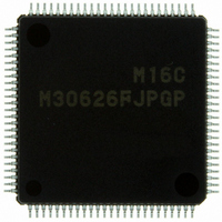
Manufacturer Part Number
M30626FJPGP#U3C
Description
IC M16C MCU FLASH 512K 100LQFP
Manufacturer
Renesas Electronics America
Series
M16C™ M16C/60r
Datasheets
1.QSK-62P_PLUS.pdf
(103 pages)
2.M30622SAFPU5.pdf
(308 pages)
3.M30620SPGPU3C.pdf
(423 pages)
Specifications of M30626FJPGP#U3C
Core Processor
M16C/60
Core Size
16-Bit
Speed
24MHz
Connectivity
I²C, IEBus, UART/USART
Peripherals
DMA, WDT
Number Of I /o
85
Program Memory Size
512KB (512K x 8)
Program Memory Type
FLASH
Ram Size
31K x 8
Voltage - Supply (vcc/vdd)
2.7 V ~ 5.5 V
Data Converters
A/D 26x10b; D/A 2x8b
Oscillator Type
Internal
Operating Temperature
-40°C ~ 85°C
Package / Case
100-LQFP
For Use With
867-1000 - KIT QUICK START RENESAS 62PR0K33062PS001BE - R0K33062P STARTER KITR0K33062PS000BE - KIT EVAL STARTER FOR M16C/62PM3062PT3-CPE-3 - EMULATOR COMPACT M16C/62P/30P
Lead Free Status / RoHS Status
Lead free / RoHS Compliant
Eeprom Size
-
Available stocks
Company
Part Number
Manufacturer
Quantity
Price


M16C/62P Group (M16C/62P, M16C/62PT)
Rev.2.41
REJ09B0185-0241
Table 8.6
I/O ports : Function as I/O ports or peripheral function I/O pins.
NOTES:
Data Bus Width BYTE
Pin
P0_0 to P0_7
P1_0 to P1_7
P2_0
P2_1 to P2_7
P3_0
P3_1 to P3_3
P3_4 to
P3_7
P4_0 to
P4_3
P4_4
P4_5
P4_6
P4_7
P5_0
P5_1
P5_2
P5_3
P5_4
P5_5
P5_6
P5_7
PM05 to PM04 bits
1. To set the PM01 to PM00 bits are set to “01b” and the PM05 to PM04 bits are set to “11b” (multiplexed bus
2. In separate bus mode, these pins serve as the address bus.
3. If the data bus is 8 bits wide, make sure the PM02 bit is set to “0” (RD, BHE, WR).
4. When accessing the area that uses a multiplexed bus, these pins output an indeterminate value during a write.
Processor Mode
assigned to the entire CS space), apply “H” to the BYTE pin (external data bus 8 bits wide). While the CNVSS
pin is held “H” (= VCC1), do not rewrite the PM05 to PM04 bits to “11b” after reset. If the PM05 to PM04 bits are
set to “11b” during memory expansion mode, P3_1 to P3_7 and P4_0 to P4_3 become I/O ports, in which case
the accessible area for each CS is 256 bytes.
Jan 10, 2006
PM11=0
PM11=1
PM06=0
PM06=1
CS0=0
CS0=1
CS1=0
CS1=1
CS2=0
CS2=1
CS3=0
CS3=1
PM02=0
PM02=1
PM02=0
PM02=1
Pin Functions for Each Processor Mode
D0 to D7
I/O ports
A0
A1 to A7
A8
A9 to A11
A12 to A15
I/O ports
A16 to A19
I/O ports
I/O ports
CS0
I/O ports
CS1
I/O ports
CS2
I/O ports
CS3
WR
−
BHE
−
RD
BCLK
HLDA
HOLD
ALE
RDY
Page 66 of 390
(3)
(3)
8 bits
00b(separate bus) bits
“H”
Memory Expansion Mode or Microprocessor Mode
D0 to D7
D8 to D15
A0
A1 to A7
A8
WRL
WRH
16 bits
“L”
01b(CS2 is for multiplexed bus and
others are for separate bus)
10b(CS1 is for multiplexed bus and
others are for separate bus)
D0 to D7
I/O ports
A0/D0
A1 to A7
/D1 to D7
A8
−
−
(3)
(3)
8 bits
“H”
(2)
(4)
(2)
D0 to D7
D8 to D15
A0
A1 to A7
/D0 to D6
A8/D7
WRL
WRH
16 bits
(2)
“L”
(4)
(2)
(4)
11b (multiplexed
bus for the entire
space)
I/O ports
I/O ports
A0/D0
A1 to A7
/D1 to D7
A8
I/O ports
I/O ports
−
−
Expansion Mode
I/O ports
(3)
(3)
Memory
8 bits
“H”
(1)
8. Bus
Related parts for M30626FJPGP#U3C
Image
Part Number
Description
Manufacturer
Datasheet
Request
R

Part Number:
Description:
KIT STARTER FOR M16C/29
Manufacturer:
Renesas Electronics America
Datasheet:

Part Number:
Description:
KIT STARTER FOR R8C/2D
Manufacturer:
Renesas Electronics America
Datasheet:

Part Number:
Description:
R0K33062P STARTER KIT
Manufacturer:
Renesas Electronics America
Datasheet:

Part Number:
Description:
KIT STARTER FOR R8C/23 E8A
Manufacturer:
Renesas Electronics America
Datasheet:

Part Number:
Description:
KIT STARTER FOR R8C/25
Manufacturer:
Renesas Electronics America
Datasheet:

Part Number:
Description:
KIT STARTER H8S2456 SHARPE DSPLY
Manufacturer:
Renesas Electronics America
Datasheet:

Part Number:
Description:
KIT STARTER FOR R8C38C
Manufacturer:
Renesas Electronics America
Datasheet:

Part Number:
Description:
KIT STARTER FOR R8C35C
Manufacturer:
Renesas Electronics America
Datasheet:

Part Number:
Description:
KIT STARTER FOR R8CL3AC+LCD APPS
Manufacturer:
Renesas Electronics America
Datasheet:
Part Number:
Description:
KIT STARTER FOR RX610
Manufacturer:
Renesas Electronics America
Datasheet:

Part Number:
Description:
KIT STARTER FOR R32C/118
Manufacturer:
Renesas Electronics America
Datasheet:

Part Number:
Description:
KIT DEV RSK-R8C/26-29
Manufacturer:
Renesas Electronics America
Datasheet:

Part Number:
Description:
KIT STARTER FOR SH7124
Manufacturer:
Renesas Electronics America
Datasheet:

Part Number:
Description:
KIT STARTER FOR H8SX/1622
Manufacturer:
Renesas Electronics America
Datasheet:

Part Number:
Description:
KIT DEV FOR SH7203
Manufacturer:
Renesas Electronics America
Datasheet: