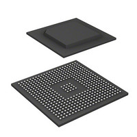
R8A77850BDBGV#RD0Z Renesas Electronics America, R8A77850BDBGV#RD0Z Datasheet - Page 180

R8A77850BDBGV#RD0Z
Manufacturer Part Number
R8A77850BDBGV#RD0Z
Description
IC SUPERH MPU ROMLESS 436BGA
Manufacturer
Renesas Electronics America
Series
SuperH® SH7780r
Datasheet
1.R8A77850AADBGV.pdf
(1694 pages)
Specifications of R8A77850BDBGV#RD0Z
Core Processor
SH-4A
Core Size
32-Bit
Speed
600MHz
Connectivity
Audio Codec, MMC, Serial Sound, SCI, SIO, SPI, SSI
Peripherals
DMA, POR, WDT
Number Of I /o
108
Program Memory Type
ROMless
Ram Size
8K x 8
Voltage - Supply (vcc/vdd)
1 V ~ 1.2 V
Oscillator Type
External
Operating Temperature
-40°C ~ 85°C
Package / Case
436-BGA
Lead Free Status / RoHS Status
Lead free / RoHS Compliant
Eeprom Size
-
Program Memory Size
-
Data Converters
-
Available stocks
Company
Part Number
Manufacturer
Quantity
Price
- Current page: 180 of 1694
- Download datasheet (9Mb)
7. Memory Management Unit (MMU)
(b) P1 Area
(c)
(d) P4 Area
Rev.1.00 Jan. 10, 2008 Page 148 of 1658
REJ09B0261-0100
The P1 area does not allow address translation using the TLB but can be accessed using the
cache.
Regardless of whether the MMU is enabled or disabled, clearing the upper 3 bits of an address
to 0 gives the corresponding physical address. Whether or not the cache is used is determined
by the CCR setting. When the cache is used, switching between the copy-back method and the
write-through method for write accesses is specified by the CB bit in CCR.
The P2 area does not allow address translation using the TLB and access using the cache.
Regardless of whether the MMU is enabled or disabled, clearing the upper 3 bits of an address
to 0 gives the corresponding physical address.
The P4 area is mapped onto the internal resource of this LSI. This area except the store queue
and on-chip memory areas does not allow address translation using the TLB. This area cannot
be accessed using the cache. The P4 area is shown in detail in figure 7.4.
P2 Area
H'E000 0000
H'E400 0000
H'E500 0000
H'E600 0000
H'F000 0000
H'F100 0000
H'F200 0000
H'F300 0000
H'F400 0000
H'F500 0000
H'F600 0000
H'F700 0000
H'F800 0000
H'FC00 0000
H'FFFF FFFF
Figure 7.4 P4 Area
Unified TLB and PMB address array
Unified TLB and PMB data array
Instruction cache address array
Operand cache address array
Instruction TLB address array
Instruction cache data array
Operand cache data array
Instruction TLB data array
On-chip memory area
Control register area
Reserved area
Reserved area
Reserved area
Store queue
Related parts for R8A77850BDBGV#RD0Z
Image
Part Number
Description
Manufacturer
Datasheet
Request
R

Part Number:
Description:
KIT STARTER FOR M16C/29
Manufacturer:
Renesas Electronics America
Datasheet:

Part Number:
Description:
KIT STARTER FOR R8C/2D
Manufacturer:
Renesas Electronics America
Datasheet:

Part Number:
Description:
R0K33062P STARTER KIT
Manufacturer:
Renesas Electronics America
Datasheet:

Part Number:
Description:
KIT STARTER FOR R8C/23 E8A
Manufacturer:
Renesas Electronics America
Datasheet:

Part Number:
Description:
KIT STARTER FOR R8C/25
Manufacturer:
Renesas Electronics America
Datasheet:

Part Number:
Description:
KIT STARTER H8S2456 SHARPE DSPLY
Manufacturer:
Renesas Electronics America
Datasheet:

Part Number:
Description:
KIT STARTER FOR R8C38C
Manufacturer:
Renesas Electronics America
Datasheet:

Part Number:
Description:
KIT STARTER FOR R8C35C
Manufacturer:
Renesas Electronics America
Datasheet:

Part Number:
Description:
KIT STARTER FOR R8CL3AC+LCD APPS
Manufacturer:
Renesas Electronics America
Datasheet:

Part Number:
Description:
KIT STARTER FOR RX610
Manufacturer:
Renesas Electronics America
Datasheet:

Part Number:
Description:
KIT STARTER FOR R32C/118
Manufacturer:
Renesas Electronics America
Datasheet:

Part Number:
Description:
KIT DEV RSK-R8C/26-29
Manufacturer:
Renesas Electronics America
Datasheet:

Part Number:
Description:
KIT STARTER FOR SH7124
Manufacturer:
Renesas Electronics America
Datasheet:

Part Number:
Description:
KIT STARTER FOR H8SX/1622
Manufacturer:
Renesas Electronics America
Datasheet:

Part Number:
Description:
KIT DEV FOR SH7203
Manufacturer:
Renesas Electronics America
Datasheet:


