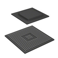
R8A77850BDBGV#RD0Z Renesas Electronics America, R8A77850BDBGV#RD0Z Datasheet - Page 222

R8A77850BDBGV#RD0Z
Manufacturer Part Number
R8A77850BDBGV#RD0Z
Description
IC SUPERH MPU ROMLESS 436BGA
Manufacturer
Renesas Electronics America
Series
SuperH® SH7780r
Datasheet
1.R8A77850AADBGV.pdf
(1694 pages)
Specifications of R8A77850BDBGV#RD0Z
Core Processor
SH-4A
Core Size
32-Bit
Speed
600MHz
Connectivity
Audio Codec, MMC, Serial Sound, SCI, SIO, SPI, SSI
Peripherals
DMA, POR, WDT
Number Of I /o
108
Program Memory Type
ROMless
Ram Size
8K x 8
Voltage - Supply (vcc/vdd)
1 V ~ 1.2 V
Oscillator Type
External
Operating Temperature
-40°C ~ 85°C
Package / Case
436-BGA
Lead Free Status / RoHS Status
Lead free / RoHS Compliant
Eeprom Size
-
Program Memory Size
-
Data Converters
-
Available stocks
Company
Part Number
Manufacturer
Quantity
Price
- Current page: 222 of 1694
- Download datasheet (9Mb)
7. Memory Management Unit (MMU)
7.7
To enable the ITLB and UTLB to be managed by software, their contents are allowed to be read
from and written to by a program in the P1/P2 area with a MOV instruction in privileged mode.
Operation is not guaranteed if access is made from a program in another area.
After the memory-mapped TLB has been accessed, execute one of the following three methods
before an access (including an instruction fetch) to an area other than the P1/P2 area is performed.
1. Execute a branch using the RTE instruction. In this case, the branch destination may be an area
2. Execute the ICBI instruction for any address (including non-cacheable area).
3. If the MT bit in IRMCR is 0 (initial value) before accessing the memory-mapped TLB, the
Note that the method 3 may not be guaranteed in the future SuperH Series. Therefore, it is
recommended that the method 1 or 2 should be used for being compatible with the future SuperH
Series.
The ITLB and UTLB are allocated to the P4 area in the virtual address space.
In TLB compatible mode, VPN, V, and ASID in the ITLB can be accessed as an address array,
PPN, V, SZ, PR, C, and SH as a data array. VPN, D, V, and ASID in the UTLB can be accessed as
an address array, PPN, V, SZ, PR, C, D, WT, and SH as a data array. V and D can be accessed
from both the address array side and the data array side.
In TLB extended mode, VPN, V, and ASID in the ITLB can be accessed as an address array, PPN,
V, ESZ, EPR, C, and SH as a data array. VPN, D, V, and ASID in the UTLB can be accessed as
an address array, PPN, V, ESZ, EPR, C, D, WT, and SH as a data array. V and D can be accessed
from both the address array side and the data array side.
In both TLB compatible mode and TLB extended mode, only longword access is possible.
Instruction fetches cannot be performed in these areas. For reserved bits, a write value of 0 should
be specified; their read value is undefined.
Rev.1.00 Jan. 10, 2008 Page 190 of 1658
REJ09B0261-0100
other than the P1/P2 area.
specific instruction does not need to be executed. However, note that the CPU processing
performance will be lowered because the instruction fetch is performed again for the next
instruction after MMUCR has been updated.
Memory-Mapped TLB Configuration
Related parts for R8A77850BDBGV#RD0Z
Image
Part Number
Description
Manufacturer
Datasheet
Request
R

Part Number:
Description:
KIT STARTER FOR M16C/29
Manufacturer:
Renesas Electronics America
Datasheet:

Part Number:
Description:
KIT STARTER FOR R8C/2D
Manufacturer:
Renesas Electronics America
Datasheet:

Part Number:
Description:
R0K33062P STARTER KIT
Manufacturer:
Renesas Electronics America
Datasheet:

Part Number:
Description:
KIT STARTER FOR R8C/23 E8A
Manufacturer:
Renesas Electronics America
Datasheet:

Part Number:
Description:
KIT STARTER FOR R8C/25
Manufacturer:
Renesas Electronics America
Datasheet:

Part Number:
Description:
KIT STARTER H8S2456 SHARPE DSPLY
Manufacturer:
Renesas Electronics America
Datasheet:

Part Number:
Description:
KIT STARTER FOR R8C38C
Manufacturer:
Renesas Electronics America
Datasheet:

Part Number:
Description:
KIT STARTER FOR R8C35C
Manufacturer:
Renesas Electronics America
Datasheet:

Part Number:
Description:
KIT STARTER FOR R8CL3AC+LCD APPS
Manufacturer:
Renesas Electronics America
Datasheet:

Part Number:
Description:
KIT STARTER FOR RX610
Manufacturer:
Renesas Electronics America
Datasheet:

Part Number:
Description:
KIT STARTER FOR R32C/118
Manufacturer:
Renesas Electronics America
Datasheet:

Part Number:
Description:
KIT DEV RSK-R8C/26-29
Manufacturer:
Renesas Electronics America
Datasheet:

Part Number:
Description:
KIT STARTER FOR SH7124
Manufacturer:
Renesas Electronics America
Datasheet:

Part Number:
Description:
KIT STARTER FOR H8SX/1622
Manufacturer:
Renesas Electronics America
Datasheet:

Part Number:
Description:
KIT DEV FOR SH7203
Manufacturer:
Renesas Electronics America
Datasheet:


