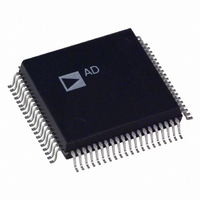
AD1843JS Analog Devices Inc, AD1843JS Datasheet - Page 10

AD1843JS
Manufacturer Part Number
AD1843JS
Description
IC CODEC STEREO 5V 16BIT 80PQFP
Manufacturer
Analog Devices Inc
Type
Stereo Audior
Datasheet
1.AD1843JS.pdf
(64 pages)
Specifications of AD1843JS
Rohs Status
RoHS non-compliant
Data Interface
Serial
Resolution (bits)
16 b
Number Of Adcs / Dacs
1 / 2
Sigma Delta
Yes
S/n Ratio, Adcs / Dacs (db) Typ
92 / 86
Dynamic Range, Adcs / Dacs (db) Typ
85 / 80
Voltage - Supply, Analog
4.75 V ~ 5.25 V
Voltage - Supply, Digital
2.85 V ~ 5.25 V
Operating Temperature
0°C ~ 70°C
Mounting Type
Surface Mount
Package / Case
80-MQFP, 80-PQFP
Available stocks
Company
Part Number
Manufacturer
Quantity
Price
Part Number:
AD1843JS
Manufacturer:
ADI/亚德诺
Quantity:
20 000
AD1843
Miscellaneous
Pin Name
XTALI
XTALO
PWRDWN
RESET
PDMNFT
CMOUT
V
FILTL
FILTR
AAFILTL
AAFILTR
REF
49
23
24
22
52
38
39
25
PQFP
61
62
51
76
TQFP
77
64
65
61
47
48
31
29
30
28
I/O
I
O
I
I
I
O
I
I
I
I
I
Description
24.576 MHz Crystal Input. When using a crystal as the clock source, the crystal
should be connected between the XTALI and XTALO pins. This crystal should
be 24.576 MHz for the normal sampling rate range, i.e., 4 kHz to 54 kHz. A
clock input (perhaps the CLKOUT of another AD1843) may be driven into
XTALI in place of a crystal. The external clock input must be greater than or equal
to 512 times the maximum desired AD1843 sampling frequency.
24.576 MHz Crystal Output. When using a crystal as the clock source, the crystal
should be connected between the XTALI and XTALO pins. If a clock is driven
directly into XTALI, then XTALO should be left unconnected.
Power Down. PWRDWN is active LO. The assertion of this signal will initialize
the on-chip Control Registers to their default values, and will completely and
quietly power down the AD1843. If a crystal is not connected between XTALI
and XTALO, there must be a 24.576 MHz clock input on XTALI for at least
5 ms after this signal is asserted LO for proper operation. The AD1843 will not
be completely powered down until after this 5 ms period elapses. The AD1843
always finishes an in-progress power-up sequence before initiating a power-down
sequence, and vice versa. If the PWRDWN pin is asserted while a power-up sequence
is in progress, the 24.576 MHz clock signal on XTALI must persist for a worst
case maximum of 479 ms (power up = 470 ms, autocalibration = 4 ms, power
down = 5 ms) after PWRDWN is asserted. When INIT (Control Register
Address 0, Bit 15) is set to a “1,” the power-down sequence is complete. See
the “Power Management” section for important additional details.
Reset. RESET is active LO. The assertion of this signal will initialize the on-chip
registers to their default values, and will completely power down the AD1843.
RESET is similar to PWRDWN, except that when PWRDWN is asserted, power
down is “quiet” and performed synchronously to the internal clocks. When RESET
is asserted, power down is “noisy” and performed asynchronously to the internal
clocks.
Power-Down Mono Feedthrough. When the AD1843 mixer is powered down,
and PDMNFT is asserted HI, the Mono Input (MIN, PQFP Pin 19) is routed to
the Mono Output (MOUT, PQFP Pin 35), and the signal applied to MIN will
feedthrough to MOUT. When the AD1843 mixer is powered down and
PDMNFT is deasserted LO, the feedthrough of MIN to MOUT will be muted.
When the AD1843 mixer is not powered down, and MIN to MOUT feedthrough
is desired, the Mono Input Mix Mute (Control Register Address 8, Bit 15) and the
Mono Output Mute (Control Register Address 8, Bit 6) must be unmuted. During
power-down feedthrough, the signal applied to the MIN input appears only at
the MOUT output. During normal operation, the signal applied to the MIN
input appears at both the MOUT and the LOUT1 outputs. The state of the
PDMNFT pin should be changed when the AD1843 mixer is powered up. If the
state of PDMNFT is changed when the AD1843 is in total power-down, audible
pops and clicks will likely result.
Common-Mode Voltage Output. Nominal 2.25 volt reference available externally
for dc-coupling and level-shifting. CMOUT should not be used where it will sink
or source current.
Voltage Reference Filter. Voltage reference filter point for external bypassing only.
Left Channel Filter. This pin requires a 1.0 F capacitor to analog ground for
proper operation.
Right Channel Filter. This pin requires a 1.0 F capacitor to analog ground for
proper operation.
Left Channel Antialias Filter. This pin requires a 1000 pF capacitor to analog
ground for proper operation.
Right Channel Antialias Filter. This pin requires a 1000 pF capacitor to analog
ground for proper operation.
–10–
REV. 0


