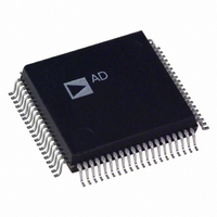
AD1843JS Analog Devices Inc, AD1843JS Datasheet - Page 9

AD1843JS
Manufacturer Part Number
AD1843JS
Description
IC CODEC STEREO 5V 16BIT 80PQFP
Manufacturer
Analog Devices Inc
Type
Stereo Audior
Datasheet
1.AD1843JS.pdf
(64 pages)
Specifications of AD1843JS
Rohs Status
RoHS non-compliant
Data Interface
Serial
Resolution (bits)
16 b
Number Of Adcs / Dacs
1 / 2
Sigma Delta
Yes
S/n Ratio, Adcs / Dacs (db) Typ
92 / 86
Dynamic Range, Adcs / Dacs (db) Typ
85 / 80
Voltage - Supply, Analog
4.75 V ~ 5.25 V
Voltage - Supply, Digital
2.85 V ~ 5.25 V
Operating Temperature
0°C ~ 70°C
Mounting Type
Surface Mount
Package / Case
80-MQFP, 80-PQFP
Available stocks
Company
Part Number
Manufacturer
Quantity
Price
Part Number:
AD1843JS
Manufacturer:
ADI/亚德诺
Quantity:
20 000
REV. 0
Analog Signals
Pin Name
LINLP
LINLN
LINRP
LINRN
MICL
MICR
AUX1L
AUX1R
AUX2L
AUX2R
AUX3L
AUX3R
MIN
MOUT
LOUT1L
LOUT1R
HPOUTL
HPOUTC
HPOUTR
LOUT2LP
LOUT2LN
LOUT2RP
LOUT2RN
SUML
SUMR
Clocks
Pin Name
CLKOUT
SYNC[3:1]
CONV[3:1] 75, 71, 67
BIT[3:1]
PQFP
76
57, 56, 55
74, 70, 66
PQFP
28
29
26
27
18
17
16
15
14
13
12
11
19
35
36
34
47
46
45
32
33
30
31
43
42
TQFP
95
71, 70, 69
94, 89, 84
92, 87, 82
TQFP
35
36
33
34
21
22
20
19
18
17
16
15
23
44
45
43
58
57
56
40
41
38
39
54
53
I/O
O
I
O
O
I/O
I
I
I
I
I
I
I
I
I
I
I
I
I
O
O
O
O
O
O
O
O
O
I
I
Description
Clock Output. This signal is a buffered version of XTALO (with a duty cycle
restored to at least 60%/40%), the crystal clock output. This pin is enabled by
default but can be three-stated by programming a bit in Control Register
Address 28. The CLKOUT frequency is 24.576 MHz.
Conversion Clock Outputs. These output clocks have an average period equal to (or 128
Bit Clock Outputs. These output clocks can be individually programmed to
programming bits in Control Register Address 28.
Sync Inputs. These SYNC signals are used as the clock source inputs to three
receptive PLLs in the AD1843. These pins accept a clock at, or at a multiple of,
the desired sample rate for A-to-D and D-to-A conversions. These inputs are
ignored if a sample rate is programmed directly, but should never be left floating.
times) the internal sample rates of the AD1843. These clock outputs are three-stated
by default but can be enabled by programming bits in Control Register Address 28.
multiples of the sample rates. Support for V.34 or V.32 bit rates is available.
These clock outputs are three-stated by default but can be enabled by
Line Output #2 Right Channel Positive Differential Signal.
Line Output #2 Right Channel Negative Differential Signal.
Description
Line Input Left Channel Positive Differential Signal.
Line Input Left Channel Negative Differential Signal.
Line Input Right Channel Positive Differential Signal.
Line Input Right Channel Negative Differential Signal.
Microphone Input Left Channel. Microphone input for the left channel. This
signal can be either line level or –20 dB from line level.
Microphone Input Right Channel. Microphone input for the right channel.
This signal can be either line level or –20 dB from line level.
Auxiliary #1 Left Channel Line Input.
Auxiliary #1 Right Channel Line Input.
Auxiliary #2 Left Channel Line Input.
Auxiliary #2 Right Channel Line Input.
Auxiliary #3 Left Channel Line Input.
Auxiliary #3 Right Channel Line Input.
Monaural (Mono) Line Input.
Monaural (Mono) Line Output.
Line Output #1 Left Channel.
Line Output #1 Right Channel.
Headphone Output Left Channel.
Headphone Common Return.
Headphone Output Right Channel.
Line Output #2 Left Channel Positive Differential Signal.
Line Output #2 Left Channel Negative Differential Signal.
Mixer Line Input Left Channel.
Mixer Line Input Right Channel.
–9–
AD1843


