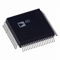
AD1843JS Analog Devices Inc, AD1843JS Datasheet - Page 22

AD1843JS
Manufacturer Part Number
AD1843JS
Description
IC CODEC STEREO 5V 16BIT 80PQFP
Manufacturer
Analog Devices Inc
Type
Stereo Audior
Datasheet
1.AD1843JS.pdf
(64 pages)
Specifications of AD1843JS
Rohs Status
RoHS non-compliant
Data Interface
Serial
Resolution (bits)
16 b
Number Of Adcs / Dacs
1 / 2
Sigma Delta
Yes
S/n Ratio, Adcs / Dacs (db) Typ
92 / 86
Dynamic Range, Adcs / Dacs (db) Typ
85 / 80
Voltage - Supply, Analog
4.75 V ~ 5.25 V
Voltage - Supply, Digital
2.85 V ~ 5.25 V
Operating Temperature
0°C ~ 70°C
Mounting Type
Surface Mount
Package / Case
80-MQFP, 80-PQFP
Available stocks
Company
Part Number
Manufacturer
Quantity
Price
Part Number:
AD1843JS
Manufacturer:
ADI/亚德诺
Quantity:
20 000
AD1843
SERIAL INTERFACE INPUT
Note that the references to slot numbers are valid only when the AD1843 is configured in master mode. For slave mode, bus owner-
ship does not necessarily start on Slot 0.
DA2V
DA1V
R/W
IA4:0
res
Format for the input data to written to the addressed Control Register. MSB is first.
Data format may be 8-bit unsigned linear PCM, 16-bit signed linear PCM, 8-bit -Law companded, or 8-bit A-Law companded.
MSB is first. DATA7:0 are ignored in 8-bit linear or 8-bit companded modes.
Control Word Input (Slot 0 or 16)
Control Register Write Data Input (Slot 1 or 17)
DAC1 Left Sample Input (Slot 2 or 18)
DATA15
DATA15
Data 15
Data 15
Data 15
DATA7
DATA7
Data 7
Data 7
Data 7
R/W
res
DAC2 Input Valid Flag. When in DAC2 stereo mode, setting this bit to “1” indicates that slots 4 and 5
DAC1 Input Valid Flag. When in DAC1 stereo mode, setting this bit to “1” indicates that slots 2 and 3
Control Register address for read or write.
contain valid playback data for the left and right channels of DAC2, respectively. When in DAC2 mono
mode, setting this bit to “1” indicates that slot 4 contains valid playback data for both left and right channels
of DAC2. Slot 5 is ignored in DAC2 mono mode. When this bit is reset to “0,” data in slots 4 and 5 is
ignored. This bit is ignored if the AD1843 did not request data for DAC2 in the last frame (see the DA2RQ
bit in the Status Word Output).
contain valid playback data for the left and right channels of DAC1, respectively. When in DAC1 mono
mode, setting this bit to “1” indicates that slot 2 contains valid playback data for both left and right channels
of DAC1. Slot 3 is ignored in DAC1 mono mode. When this bit is reset to “0,” data in slots 2 and 3 is
ignored. This bit is ignored if the AD1843 did not request data for DAC1 in the last frame (see the DA1RQ
bit in the Status Word Output).
Read/Write Request. Either a read from or a write to a Control Register occurs every frame. Setting this bit
to “1” indicates a Control Register read while resetting this bit to “0” initiates a Control Register write. Bits
IA4:0 define the Control Register address. When reading, the contents of the Control Register addressed are
transmitted during slot 1 of the following frame. When writing, the data to be written is taken from slot 1
and the former contents of the Control Register are transmitted during slot 1 of the following frame.
Reserved for future expansion. To ensure future compatibility, write “0” to all reserved bits.
DATA14
DATA14
Data 14
Data 14
Data 14
DATA6
DATA6
Data 6
Data 6
Data 6
res
res
DATA13
DATA13
Data 13
Data 13
Data 13
DATA5
DATA5
Data 5
Data 5
Data 5
res
res
DATA12
DATA12
Data 12
Data 12
Data 12
DATA4
DATA4
Data 4
Data 4
Data 4
IA4
res
–22–
DATA11
DATA11
Data 11
DATA3
Data 11
Data 11
DATA3
Data 3
Data 3
Data 3
IA3
res
DATA10
DATA10
Data 10
DATA2
Data 10
Data 10
DATA2
Data 2
Data 2
Data 2
IA2
res
DATA9
DATA1
DATA9
DATA1
Data 9
Data 1
Data 9
Data 1
Data 9
Data 1
DA2V
IA1
DATA8
DATA0
DATA8
DATA0
Data 8
Data 0
Data 8
Data 0
Data 8
Data 0
DA1V
IA0
REV. 0


