AD1843JS Analog Devices Inc, AD1843JS Datasheet - Page 37
AD1843JS
Manufacturer Part Number
AD1843JS
Description
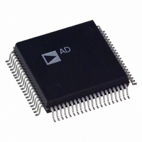
IC CODEC STEREO 5V 16BIT 80PQFP
Manufacturer
Analog Devices Inc
Type
Stereo Audior
Datasheet
1.AD1843JS.pdf
(64 pages)
Specifications of AD1843JS
Rohs Status
RoHS non-compliant
Data Interface
Serial
Resolution (bits)
16 b
Number Of Adcs / Dacs
1 / 2
Sigma Delta
Yes
S/n Ratio, Adcs / Dacs (db) Typ
92 / 86
Dynamic Range, Adcs / Dacs (db) Typ
85 / 80
Voltage - Supply, Analog
4.75 V ~ 5.25 V
Voltage - Supply, Digital
2.85 V ~ 5.25 V
Operating Temperature
0°C ~ 70°C
Mounting Type
Surface Mount
Package / Case
80-MQFP, 80-PQFP
Available stocks
Company
Part Number
Manufacturer
Quantity
Price

Part Number:
AD1843JS
Manufacturer:
ADI/亚德诺
Quantity:
20 000


REV. 0
DA2C1:0
DA1C1:0
ADRC1:0
ADLC1:0
res
C1REF
Address 15
Address 16
Data 15
Data 15
C1REF
Data 7
Data 7
C1M7
res
res
DAC2 Sample Rate Source. Selects the sample rate clock source for left and right channels of DAC2.
00 = Conversion Sample Rate is 48.0 kHz
01 = Conversion Sample Rate is from Clock Generator 1
10 = Conversion Sample Rate is from Clock Generator 2
11 = Conversion Sample Rate is from Clock Generator 3
DAC1 Sample Rate Source. Selects the sample rate clock source for left and right channels of DAC1.
00 = Conversion Sample Rate is 48.0 kHz
01 = Conversion Sample Rate is from Clock Generator 1
10 = Conversion Sample Rate is from Clock Generator 2
11 = Conversion Sample Rate is from Clock Generator 3
ADC Right Sample Rate Source. Selects the sample rate clock source for the right ADC channel.
00 = Conversion Sample Rate is 48.0 kHz
01 = Conversion Sample Rate is from Clock Generator 1
01 = Conversion Sample Rate is from Clock Generator 2
11 = Conversion Sample Rate is from Clock Generator 3
ADC Left Sample Rate Source. Selects the sample rate clock source for the left ADC channel.
00 = Conversion Sample Rate is 48.0 kHz
01 = Conversion Sample Rate is from Clock Generator 1
10 = Conversion Sample Rate is from Clock Generator 2
11 = Conversion Sample Rate is from Clock Generator 3
Reserved for future expansion. To ensure future compatibility, write “0” to all reserved bits.
Initial default state after reset: 0000 0000 0000 0000 (0000 hex). Cleared to default and cannot be written to when:
the RESET pin is asserted LO; when the PWRDWN pin is asserted LO; or when the PDNO bit in Control Register
Address 0 is set to “1” (all conversions disabled).
Clock Generator 1 Reference Select. Selects the fundamental clock reference used by Clock Generator 1 to
synthesize its “Conversion” (sample) and “Bit” clock rates.
0 = Clocks are referenced to the input on pin XTALI (crystal or master clock input).
1 = Clocks are referenced to the input on pin SYNC1 (Sync 1 Clock Input).
Sample clock frequency is defined by Control Register Address 17 and Bit C1X8/7.
Sample clock phase may be shifted by Control Register Address 18.
Bit clock frequency is defined by bits C1M7:0 and C1P200.
Bit C1VID is ignored.
Sample clock frequency is defined by C1VID and C1M7:0.
Sample clock phase is locked to SYNC1 and cannot be shifted.
Bit clock frequency is defined by bits C1M7:0 and C1P200 unless in Video Lock Mode (C1VID set to “1”)
where the Bit clocks are not produced.
Control Register Addresses 17, 18 and the C1X8/7 bit are ignored.
Data 14
Data 14
C1VID
Data 6
Data 6
C1M6
res
res
Codec Configuration—Channel Sample Rate Source Select
Clock Generator 1 Control—Mode
C1PLLG
Data 13
Data 13
Data 5
Data 5
C1M5
res
res
Data 12
Data 12
C1P200
Data 4
Data 4
C1M4
res
res
–37–
Data 11
Data 11
DA2C1
ADRC1
C1X8/7
Data 3
Data 3
C1M3
Data 10
Data 10
C1C128
DA2C0
ADRC0
Data 2
Data 2
C1M2
DA1C1
ADLC1
Data 9
Data 1
Data 9
Data 1
C1M1
res
ADLC0
DA1C0
Data 8
Data 0
Data 8
Data 0
C1M0
AD1843
res
Related parts for AD1843JS
Image
Part Number
Description
Manufacturer
Datasheet
Request
R

Part Number:
Description:
±1.7g Dual-Axis IMEMS Accelerometer Evaluation Board
Manufacturer:
Analog Devices Inc
Datasheet:

Part Number:
Description:
Inertial Sensor Evaluation System
Manufacturer:
Analog Devices Inc
Datasheet:
Part Number:
Description:
Manufacturer:
Analog Devices Inc
Datasheet:
Part Number:
Description:
Manufacturer:
Analog Devices Inc
Datasheet:
Part Number:
Description:
Manufacturer:
Analog Devices Inc
Datasheet:
Part Number:
Description:
Manufacturer:
Analog Devices Inc
Datasheet:
Part Number:
Description:
Manufacturer:
Analog Devices Inc
Datasheet:
Part Number:
Description:
Manufacturer:
Analog Devices Inc
Datasheet:
Part Number:
Description:
Manufacturer:
Analog Devices Inc
Datasheet:
Part Number:
Description:
Manufacturer:
Analog Devices Inc
Datasheet:
Part Number:
Description:
Manufacturer:
Analog Devices Inc
Datasheet:
Part Number:
Description:
Manufacturer:
Analog Devices Inc
Datasheet:
Part Number:
Description:
Manufacturer:
Analog Devices Inc
Datasheet: