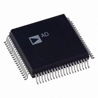
AD1843JS Analog Devices Inc, AD1843JS Datasheet - Page 25

AD1843JS
Manufacturer Part Number
AD1843JS
Description
IC CODEC STEREO 5V 16BIT 80PQFP
Manufacturer
Analog Devices Inc
Type
Stereo Audior
Datasheet
1.AD1843JS.pdf
(64 pages)
Specifications of AD1843JS
Rohs Status
RoHS non-compliant
Data Interface
Serial
Resolution (bits)
16 b
Number Of Adcs / Dacs
1 / 2
Sigma Delta
Yes
S/n Ratio, Adcs / Dacs (db) Typ
92 / 86
Dynamic Range, Adcs / Dacs (db) Typ
85 / 80
Voltage - Supply, Analog
4.75 V ~ 5.25 V
Voltage - Supply, Digital
2.85 V ~ 5.25 V
Operating Temperature
0°C ~ 70°C
Mounting Type
Surface Mount
Package / Case
80-MQFP, 80-PQFP
Available stocks
Company
Part Number
Manufacturer
Quantity
Price
Part Number:
AD1843JS
Manufacturer:
ADI/亚德诺
Quantity:
20 000
REV. 0
res
res
CONTROL REGISTERS
Control Register Architecture
All Control Registers are cleared to their default state when either the RESET pin or the PWRDWN pin is asserted. All conversion
related Control Registers (Addresses 1–15, 25 and 27) are cleared to defaults when the conversion resources of the AD1843 are pow-
ered down through the PDNI bit in Control Register Address 28. Control Registers which manage analog DAC gain/attenuation
(Addresses 3–10) are cleared to defaults whenever the resource they manage is powered down. Finally, the three clock generator
sample phase shift Control Registers (Addresses 18, 21 and 24) are cleared to defaults whenever their associated clock generator is
powered down. Writes to Control Registers are blocked until a clearing condition no longer exists. Writes to Control Registers are
also blocked immediately after the RESET pin or the PWRDWN pin is asserted until the AD1843’s internal clocks have settled,
which is indicated by the INIT bit in Control Register Address 0. Control Registers may always be read.
Figures 12 and 13 associate the Control Registers to the AD1843 Block Diagram.
Reserved Output (Slots 4 or 20)
Reserved Output (Slots 5 or 21)
Data 15
Data 15
Data 7
Data 7
res
res
res
res
Reserved for future expansion. Read back as “0.” Should be ignored to ensure future compatibility.
Reserved for future expansion. Read back as “0.” Should be ignored to ensure future compatibility.
Data 14
Data 14
Data 6
Data 6
res
res
res
res
Data 13
Data 13
Data 5
Data 5
res
res
res
res
Data 12
Data 12
Data 4
Data 4
res
res
res
res
–25–
Data 11
Data 11
Data 3
Data 3
res
res
res
res
Data 10
Data 10
Data 2
Data 2
res
res
res
res
Data 9
Data 1
Data 9
Data 1
res
res
res
res
Data 8
Data 0
Data 8
Data 0
AD1843
res
res
res
res


