AD1843JS Analog Devices Inc, AD1843JS Datasheet - Page 42
AD1843JS
Manufacturer Part Number
AD1843JS
Description
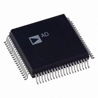
IC CODEC STEREO 5V 16BIT 80PQFP
Manufacturer
Analog Devices Inc
Type
Stereo Audior
Datasheet
1.AD1843JS.pdf
(64 pages)
Specifications of AD1843JS
Rohs Status
RoHS non-compliant
Data Interface
Serial
Resolution (bits)
16 b
Number Of Adcs / Dacs
1 / 2
Sigma Delta
Yes
S/n Ratio, Adcs / Dacs (db) Typ
92 / 86
Dynamic Range, Adcs / Dacs (db) Typ
85 / 80
Voltage - Supply, Analog
4.75 V ~ 5.25 V
Voltage - Supply, Digital
2.85 V ~ 5.25 V
Operating Temperature
0°C ~ 70°C
Mounting Type
Surface Mount
Package / Case
80-MQFP, 80-PQFP
Available stocks
Company
Part Number
Manufacturer
Quantity
Price

Part Number:
AD1843JS
Manufacturer:
ADI/亚德诺
Quantity:
20 000


AD1843
C2C15:0
C2PD
C2P7:0
res
C3REF
Address 20
Address 21
Address 22
Data 15
Data 15
Data 15
C3REF
C2C15
Data 7
Data 7
Data 7
C3M7
C2C7
C2P7
res
Clock Generator 2 Phase Shift Direction. This bit controls the direction of sample clock phase shift.
Reserved for future expansion. To ensure future compatibility, write “0” to all reserved bits.
Clock Generator 3 Reference Select. Selects the fundamental clock reference used by Clock Generator 3 to synthe-
Clock Generator 2 Conversion (Sample) Rate Select. Defines the conversion rate produced by Clock Generator 2 when
not referenced to the SYNC2 pin (Control Register Address 19 Bit 15 [C2REF]). One LSB represents exactly one Hertz,
assuming a 24.576 MHz clock input on the XTALI pin. Usable range is 4 kHz (0x0FA0) to 54 kHz (0xD2F0).
Initial default state after reset: 1011 1011 1000 0000 (BB80 hex), which is 48 kHz, assuming a 24.576 MHz clock in-
put on the XTALI pin. Cleared to default and cannot be written to when: the RESET pin is asserted LO; or when
the PWRDWN pin is asserted LO.
0 = Phase Advance
1 = Phase Retard
Clock Generator 2 Phase Shift Magnitude. These bits control the magnitude of sample clock phase shift. One LSB repre-
sents exactly 0.12 degrees. LSBs are processed and decremented at a rate of 3.072 MHz (assuming a 24.576 MHz clock
input on the XTALI pin). When this register is read, it indicates any phase advance/retard remaining to be processed as of
the beginning of slot 0 if bus master, or when TSI was received if bus slave. This register may be overwritten even if all pre-
viously programmed phase advance/retard has not been processed. When written, the contents of this register (just prior to
the write) are transmitted during slot 1 of the following frame (as with all Control Register writes).
Initial default state after reset: 0000 0000 0000 0000 (0000 hex). Cleared to default and cannot be written to when:
the RESET pin is asserted LO; when the PWRDWN pin is asserted LO; or when the G2EN bit in Control Register
Address 28 is reset to “0” (clock generator 2 disabled).
size its “Conversion” (sample) and “Bit” clock rates.
0 = Clocks are referenced to the input on pin XTALI (crystal or master clock input).
Sample clock frequency is defined by Control Register Address 23 and Bit C3X8/7.
Sample clock phase may be shifted by Control Register Address 24.
Bit clock frequency is defined by bits C3M7:0 and C3P200.
Bit C3VID is ignored.
Data 14
Data 14
Data 14
C3VID
C2C14
Data 6
Data 6
Data 6
C3M6
C2C6
C2P6
res
Clock Generator 2 Control—Sample Phase Shift
Clock Generator 2 Control—Sample Rate
Clock Generator 3 Control—Mode
C3PLLG
Data 13
Data 13
Data 13
Data 5
C2C13
Data 5
Data 5
C3M5
C2C5
C2P5
res
Data 12
Data 12
Data 12
C3P200
Data 4
C2C12
Data 4
Data 4
C3M4
C2C4
C2P4
res
–42–
Data 11
Data 11
Data 11
C3X8/7
Data 3
C2C11
Data 3
Data 3
C3M3
C2C3
C2P3
res
Data 10
Data 10
Data 10
C3C128
Data 2
C2C10
Data 2
Data 2
C3M2
C2P2
C2C2
res
Data 9
Data 1
Data 9
Data 1
Data 9
Data 1
C3M1
C2P1
C2C9
C2C1
res
res
Data 8
Data 0
Data 8
Data 0
C2PD
Data 8
Data 0
C2P0
C3M0
C2C8
C2C0
res
REV. 0
Related parts for AD1843JS
Image
Part Number
Description
Manufacturer
Datasheet
Request
R

Part Number:
Description:
±1.7g Dual-Axis IMEMS Accelerometer Evaluation Board
Manufacturer:
Analog Devices Inc
Datasheet:

Part Number:
Description:
Inertial Sensor Evaluation System
Manufacturer:
Analog Devices Inc
Datasheet:
Part Number:
Description:
Manufacturer:
Analog Devices Inc
Datasheet:
Part Number:
Description:
Manufacturer:
Analog Devices Inc
Datasheet:
Part Number:
Description:
Manufacturer:
Analog Devices Inc
Datasheet:
Part Number:
Description:
Manufacturer:
Analog Devices Inc
Datasheet:
Part Number:
Description:
Manufacturer:
Analog Devices Inc
Datasheet:
Part Number:
Description:
Manufacturer:
Analog Devices Inc
Datasheet:
Part Number:
Description:
Manufacturer:
Analog Devices Inc
Datasheet:
Part Number:
Description:
Manufacturer:
Analog Devices Inc
Datasheet:
Part Number:
Description:
Manufacturer:
Analog Devices Inc
Datasheet:
Part Number:
Description:
Manufacturer:
Analog Devices Inc
Datasheet:
Part Number:
Description:
Manufacturer:
Analog Devices Inc
Datasheet: