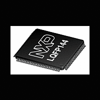
LPC2917_19_01 NXP Semiconductors, LPC2917_19_01 Datasheet - Page 11

LPC2917_19_01
Manufacturer Part Number
LPC2917_19_01
Description
The LPC2917/2919/01 combine an ARM968E-S CPU core with two integrated TCMblocks operating at frequencies of up to 125 MHz, CAN and LIN, 56 kB SRAM, up to768 kB flash memory, external memory interface, two 10-bit ADCs, and multiple serial andparallel
Manufacturer
NXP Semiconductors
Datasheet
1.LPC2917_19_01.pdf
(86 pages)
- Current page: 11 of 86
- Download datasheet (555Kb)
NXP Semiconductors
Table 3.
[1]
[2]
[3]
6. Functional description
LPC2917_19_01_3
Product data sheet
Pin name
V
P0[18]/IN2[2]/
PMAT2[0]/A14
P0[19]/IN2[3]/
PMAT2[1]/A15
P3[4]/MAT3[2]/
PMAT2[4]/
TXDC1
P3[5]/MAT3[3]/
PMAT2[5]/
RXDC1
P2[18]/SCS2[1]/
PCAP1[1]/D16
P2[19]/SCS2[0]/
PCAP1[2]/D17
P0[20]/IN2[4]/
PMAT2[2]/A16
P0[21]/IN2[5]/
PMAT2[3]/A17
P0[22]/IN2[6]/
PMAT2[4]/A18
V
P0[23]/IN2[7]/
PMAT2[5]/A19
P2[20]/
PCAP2[0]/D18
TDI
DD(IO)
SS(IO)
Bidirectional pad; analog port; plain input; 3-state output; slew rate control; 5V tolerant; TTL with hysteresis; programmable pull-up /
pull-down / repeater.
Analog pad; analog I/O
Analog pad.
LQFP144 pin assignment
Pin
131
132
133
134
135
136
137
138
139
140
141
142
143
144
6.1 Architectural overview
[3]
[3]
[1]
[1]
[1]
[1]
[3]
[3]
[3]
[3]
[1]
[1]
The LPC2917/2919/01 consists of:
Description
Default function
3.3 V power supply for I/O
GPIO 0, pin 18
GPIO 0, pin 19
GPIO 3, pin 4
GPIO 3, pin 5
GPIO 2, pin 18
GPIO 2, pin 19
GPIO 0, pin 20
GPIO 0, pin 21
GPIO 0, pin 22
ground for I/O
GPIO 0, pin 23
GPIO 2, pin 20
IEEE 1149.1 data in, pulled up internally
•
•
•
An ARM968E-S processor with real-time emulation support
An AMBA multi-layer Advanced High-performance Bus (AHB) for interfacing to the
on-chip memory controllers
Two DTL buses (an universal NXP interface) for interfacing to the interrupt controller
and the Power, Clock and Reset Control cluster (also called subsystem).
…continued
Rev. 03 — 9 December 2009
Function 1
ADC2 IN2
ADC2 IN3
TIMER3 MAT2
TIMER3 MAT3
SPI2 SCS1
SPI2 SCS0
ADC2 IN4
ADC2 IN5
ADC2 IN6
ADC2 IN7
SPI2 SDO
LPC2917/01; LPC2919/01
ARM9 microcontroller with CAN and LIN
Function 2
PWM2 MAT0
PWM2 MAT1
PWM2 MAT4
PWM2 MAT5
PWM1 CAP1
PWM1 CAP2
PWM2 MAT2
PWM2 MAT3
PWM2 MAT4
PWM2 MAT5
PWM2 CAP0
Function 3
EXTBUS A14
EXTBUS A15
CAN1 TXD
CAN1 RXD
EXTBUS D16
EXTBUS D17
EXTBUS A16
EXTBUS A17
EXTBUS A18
EXTBUS A19
EXTBUS D18
© NXP B.V. 2009. All rights reserved.
11 of 86
Related parts for LPC2917_19_01
Image
Part Number
Description
Manufacturer
Datasheet
Request
R

Part Number:
Description:
ARM9 microcontroller with CAN and LIN
Manufacturer:
NXP [NXP Semiconductors]
Datasheet:
Part Number:
Description:
Arm9 Microcontroller With Can And Lin
Manufacturer:
NXP Semiconductors
Datasheet:
Part Number:
Description:
NXP Semiconductors designed the LPC2420/2460 microcontroller around a 16-bit/32-bitARM7TDMI-S CPU core with real-time debug interfaces that include both JTAG andembedded trace
Manufacturer:
NXP Semiconductors
Datasheet:

Part Number:
Description:
NXP Semiconductors designed the LPC2458 microcontroller around a 16-bit/32-bitARM7TDMI-S CPU core with real-time debug interfaces that include both JTAG andembedded trace
Manufacturer:
NXP Semiconductors
Datasheet:
Part Number:
Description:
NXP Semiconductors designed the LPC2468 microcontroller around a 16-bit/32-bitARM7TDMI-S CPU core with real-time debug interfaces that include both JTAG andembedded trace
Manufacturer:
NXP Semiconductors
Datasheet:
Part Number:
Description:
NXP Semiconductors designed the LPC2470 microcontroller, powered by theARM7TDMI-S core, to be a highly integrated microcontroller for a wide range ofapplications that require advanced communications and high quality graphic displays
Manufacturer:
NXP Semiconductors
Datasheet:
Part Number:
Description:
NXP Semiconductors designed the LPC2478 microcontroller, powered by theARM7TDMI-S core, to be a highly integrated microcontroller for a wide range ofapplications that require advanced communications and high quality graphic displays
Manufacturer:
NXP Semiconductors
Datasheet:
Part Number:
Description:
The Philips Semiconductors XA (eXtended Architecture) family of 16-bit single-chip microcontrollers is powerful enough to easily handle the requirements of high performance embedded applications, yet inexpensive enough to compete in the market for hi
Manufacturer:
NXP Semiconductors
Datasheet:
Part Number:
Description:
The XA-S3 device is a member of Philips Semiconductors? XA(eXtended Architecture) family of high performance 16-bitsingle-chip microcontrollers
Manufacturer:
NXP Semiconductors
Datasheet:

Part Number:
Description:
The NXP BlueStreak LH75401/LH75411 family consists of two low-cost 16/32-bit System-on-Chip (SoC) devices
Manufacturer:
NXP Semiconductors
Datasheet:

Part Number:
Description:
The NXP LPC3130/3131 combine an 180 MHz ARM926EJ-S CPU core, high-speed USB2
Manufacturer:
NXP Semiconductors
Datasheet:

Part Number:
Description:
The NXP LPC3141 combine a 270 MHz ARM926EJ-S CPU core, High-speed USB 2
Manufacturer:
NXP Semiconductors

Part Number:
Description:
The NXP LPC3143 combine a 270 MHz ARM926EJ-S CPU core, High-speed USB 2
Manufacturer:
NXP Semiconductors

Part Number:
Description:
The NXP LPC3152 combines an 180 MHz ARM926EJ-S CPU core, High-speed USB 2
Manufacturer:
NXP Semiconductors


