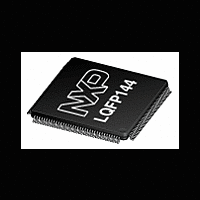
LPC2917_19_01 NXP Semiconductors, LPC2917_19_01 Datasheet - Page 41

LPC2917_19_01
Manufacturer Part Number
LPC2917_19_01
Description
The LPC2917/2919/01 combine an ARM968E-S CPU core with two integrated TCMblocks operating at frequencies of up to 125 MHz, CAN and LIN, 56 kB SRAM, up to768 kB flash memory, external memory interface, two 10-bit ADCs, and multiple serial andparallel
Manufacturer
NXP Semiconductors
Datasheet
1.LPC2917_19_01.pdf
(86 pages)
- Current page: 41 of 86
- Download datasheet (555Kb)
NXP Semiconductors
LPC2917_19_01_3
Product data sheet
6.14.4.3 Clock description
6.14.5 Pulse Width Modulator (PWM)
Table 22.
Remark: Note that the ADC1 and ADC2 accept an input voltage up to of 3.6 V (see
Table
The ADC modules are clocked from two different sources; CLK_MSCSS_ADCx_APB and
CLK_ADCx (x = 1 or 2), see
and CLK_MSCSS_ADCx_APB branch clocks for power management. If an ADC is
unused both its CLK_MSCSS_ADCx_APB and CLK_ADCx can be switched off.
The frequency of all the CLK_MSCSS_ADCx_APB clocks is identical to
CLK_MSCSS_APB since they are derived from the same base clock
BASE_MSCSS_CLK. Likewise the frequency of all the CLK_ADCx clocks is identical
since they are derived from the same base clock BASE_ADC_CLK.
The register interface towards the system bus is clocked by CLK_MSCSS_ADCx_APB.
Control logic for the analog section of the ADC is clocked by CLK_ADCx, see also
Figure
The MSCSS in the LPC2917/2919/01 includes four PWM modules with the following
features.
Symbol
ADC1/2 IN[7:0]
ADCn_EXT_START CAP1[n]
VREFN
VREFP
•
•
•
•
•
•
•
•
•
•
Six pulse-width modulated output signals
Double edge features (rising and falling edges programmed individually)
Optional interrupt generation on match (each edge)
Different operation modes: continuous or run-once
16-bit PWM counter and 16-bit prescale counter allow a large range of PWM periods
A protective mode (TRAP) holding the output in a software-controllable state and with
optional interrupt generation on a trap event
Three capture registers and capture trigger pins with optional interrupt generation on
a capture event
Interrupt generation on match event, capture event, PWM counter overflow or trap
event
A burst mode mixing the external carrier signal with internally generated PWM
Programmable sync-delay output to trigger other PWM modules (master/slave
behavior)
33) on the ADC1/2 IN pins. If the ADC is not used, the pins are 5 V tolerant.
9.
Analog to digital converter pins
Pin name
IN1/2[7:0]
VREFN
VREFP
Rev. 03 — 9 December 2009
Section
Direction
IN
IN
IN
IN
LPC2917/01; LPC2919/01
6.7.2. Note that each ADC has its own CLK_ADCx
Description
analog input for 3.3 V ADC1/2, channel 7 to
channel 0
ADC external start-trigger input (n = 1 or 2)
ADC LOW reference level
ADC HIGH reference level
ARM9 microcontroller with CAN and LIN
© NXP B.V. 2009. All rights reserved.
41 of 86
Related parts for LPC2917_19_01
Image
Part Number
Description
Manufacturer
Datasheet
Request
R

Part Number:
Description:
ARM9 microcontroller with CAN and LIN
Manufacturer:
NXP [NXP Semiconductors]
Datasheet:
Part Number:
Description:
Arm9 Microcontroller With Can And Lin
Manufacturer:
NXP Semiconductors
Datasheet:
Part Number:
Description:
NXP Semiconductors designed the LPC2420/2460 microcontroller around a 16-bit/32-bitARM7TDMI-S CPU core with real-time debug interfaces that include both JTAG andembedded trace
Manufacturer:
NXP Semiconductors
Datasheet:

Part Number:
Description:
NXP Semiconductors designed the LPC2458 microcontroller around a 16-bit/32-bitARM7TDMI-S CPU core with real-time debug interfaces that include both JTAG andembedded trace
Manufacturer:
NXP Semiconductors
Datasheet:
Part Number:
Description:
NXP Semiconductors designed the LPC2468 microcontroller around a 16-bit/32-bitARM7TDMI-S CPU core with real-time debug interfaces that include both JTAG andembedded trace
Manufacturer:
NXP Semiconductors
Datasheet:
Part Number:
Description:
NXP Semiconductors designed the LPC2470 microcontroller, powered by theARM7TDMI-S core, to be a highly integrated microcontroller for a wide range ofapplications that require advanced communications and high quality graphic displays
Manufacturer:
NXP Semiconductors
Datasheet:
Part Number:
Description:
NXP Semiconductors designed the LPC2478 microcontroller, powered by theARM7TDMI-S core, to be a highly integrated microcontroller for a wide range ofapplications that require advanced communications and high quality graphic displays
Manufacturer:
NXP Semiconductors
Datasheet:
Part Number:
Description:
The Philips Semiconductors XA (eXtended Architecture) family of 16-bit single-chip microcontrollers is powerful enough to easily handle the requirements of high performance embedded applications, yet inexpensive enough to compete in the market for hi
Manufacturer:
NXP Semiconductors
Datasheet:
Part Number:
Description:
The XA-S3 device is a member of Philips Semiconductors? XA(eXtended Architecture) family of high performance 16-bitsingle-chip microcontrollers
Manufacturer:
NXP Semiconductors
Datasheet:

Part Number:
Description:
The NXP BlueStreak LH75401/LH75411 family consists of two low-cost 16/32-bit System-on-Chip (SoC) devices
Manufacturer:
NXP Semiconductors
Datasheet:

Part Number:
Description:
The NXP LPC3130/3131 combine an 180 MHz ARM926EJ-S CPU core, high-speed USB2
Manufacturer:
NXP Semiconductors
Datasheet:

Part Number:
Description:
The NXP LPC3141 combine a 270 MHz ARM926EJ-S CPU core, High-speed USB 2
Manufacturer:
NXP Semiconductors

Part Number:
Description:
The NXP LPC3143 combine a 270 MHz ARM926EJ-S CPU core, High-speed USB 2
Manufacturer:
NXP Semiconductors

Part Number:
Description:
The NXP LPC3152 combines an 180 MHz ARM926EJ-S CPU core, High-speed USB 2
Manufacturer:
NXP Semiconductors


