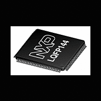
LPC2917_19_01 NXP Semiconductors, LPC2917_19_01 Datasheet - Page 20

LPC2917_19_01
Manufacturer Part Number
LPC2917_19_01
Description
The LPC2917/2919/01 combine an ARM968E-S CPU core with two integrated TCMblocks operating at frequencies of up to 125 MHz, CAN and LIN, 56 kB SRAM, up to768 kB flash memory, external memory interface, two 10-bit ADCs, and multiple serial andparallel
Manufacturer
NXP Semiconductors
Datasheet
1.LPC2917_19_01.pdf
(86 pages)
NXP Semiconductors
LPC2917_19_01_3
Product data sheet
6.8.1 Functional description
6.8 Flash memory controller
The flash memory has a 128-bit wide data interface and the flash controller offers two
128-bit buffer lines to improve system performance. The flash has to be programmed
initially via JTAG. In-system programming must be supported by the bootloader.
In-application programming is possible. Flash memory contents can be protected by
disabling JTAG access. Suspension of burning or erasing is not supported.
The Flash Memory Controller (FMC) interfaces to the embedded flash memory for two
tasks:
The key features are:
After reset, flash initialization is started, which takes t
initialization, flash access is not possible and AHB transfers to flash are stalled, blocking
the AHB bus.
During flash initialization, the index sector is read to identify the status of the JTAG access
protection and sector security. If JTAG access protection is active, the flash is not
accessible via JTAG. In this case, ARM debug facilities are disabled and flash-memory
contents cannot be read. If sector security is active, only the unsecured sections can be
read.
Flash can be read synchronously or asynchronously to the system clock. In synchronous
operation, the flash goes into standby after returning the read data. Started reads cannot
be stopped, and speculative reading and dual buffering are therefore not supported.
With asynchronous reading, transfer of the address to the flash and of read data from the
flash is done asynchronously, giving the fastest possible response time. Started reads can
be stopped, so speculative reading and dual buffering are supported.
Buffering is offered because the flash has a 128-bit wide data interface while the AHB
interface has only 32 bits. With buffering a buffer line holds the complete 128-bit flash
word, from which four words can be read. Without buffering every AHB data port read
starts a flash read. A flash read is a slow process compared to the minimum AHB cycle
time, so with buffering the average read time is reduced. This can improve system
performance.
With single buffering, the most recently read flash word remains available until the next
flash read. When an AHB data-port read transfer requires data from the same flash word
as the previous read transfer, no new flash read is done and the read data is given without
wait cycles.
•
•
•
•
•
•
Memory data transfer
Memory configuration via triggering, programming, and erasing
Programming by CPU via AHB
Programming by external programmer via JTAG
JTAG access protection
Burn-finished and erase-finished interrupt
Rev. 03 — 9 December 2009
LPC2917/01; LPC2919/01
ARM9 microcontroller with CAN and LIN
init
time (see
Section
© NXP B.V. 2009. All rights reserved.
9). During this
20 of 86


