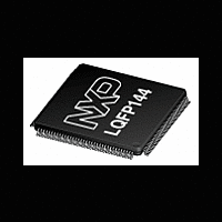
LPC2917_19_01 NXP Semiconductors, LPC2917_19_01 Datasheet - Page 62

LPC2917_19_01
Manufacturer Part Number
LPC2917_19_01
Description
The LPC2917/2919/01 combine an ARM968E-S CPU core with two integrated TCMblocks operating at frequencies of up to 125 MHz, CAN and LIN, 56 kB SRAM, up to768 kB flash memory, external memory interface, two 10-bit ADCs, and multiple serial andparallel
Manufacturer
NXP Semiconductors
Datasheet
1.LPC2917_19_01.pdf
(86 pages)
- Current page: 62 of 86
- Download datasheet (555Kb)
NXP Semiconductors
[8]
Table 34.
V
[1]
[2]
[3]
[4]
[5]
[6]
[7]
[8]
LPC2917_19_01_3
Product data sheet
Symbol
V
V
Z
V
C
E
E
E
E
E
R
DDA(ADC3V3)
Fig 16. Suggested ADC interface - LPC2917/2919/01 ADC1/2 IN[y] pin
i
VREFN
VREFP
IA
D
L(adj)
O
G
T
ia
vsi
The power-up reset has a time filter: V
V
Conditions: V
The ADC is monotonic, there are no missing codes.
The differential linearity error (E
The integral non-linearity (E
appropriate adjustment of gain and offset errors. See
The offset error (E
ideal curve. See
The gain error (E
error, and the straight line which fits the ideal transfer curve. See
The absolute error (E
ADC and the ideal transfer curve. See
See
trip(low)
Figure
for 11 μs before internal reset is asserted.
ADC static characteristics
= 3.0 V to 3.6 V; T
Parameter
voltage on pin VREFN
voltage on pin VREFP
input impedance
analog input voltage
analog input capacitance
differential linearity error
integral non-linearity
offset error
gain error
absolute error
voltage source interface
resistance
16.
SS(IO)
Figure
G
O
) is the relative difference in percent between the straight line fitting the actual transfer curve after removing offset
= 0 V, V
) is the absolute difference between the straight line which fits the actual curve and the straight line which fits the
T
) is the maximum difference between the center of the steps of the actual transfer curve of the non-calibrated
17.
DDA(ADC3V3)
L(adj)
ADC IN[y]
amb
D
) is the peak difference between the center of the steps of the actual and the ideal transfer curve after
) is the difference between the actual step width and the ideal step width. See
=
SAMPLE
−
DD(CORE)
40
Figure
= 3.3 V.
°
C to +85
Conditions
between V
V
VREFP
17.
must be above V
LPC2XXX
Rev. 03 — 9 December 2009
V
3 pF
SS(IO),
°
Figure
C unless otherwise specified; ADC frequency 4.5 MHz.
VREFN
20 kΩ
V
SS(CORE)
17.
and
trip(high)
Figure
5 pF
LPC2917/01; LPC2919/01
for 2 μs before reset is de-asserted; V
17.
[1][2][3]
[1][4]
[1][5]
[1][6]
[1][7]
[8]
ADC IN[y]
ARM9 microcontroller with CAN and LIN
Min
0
V
4.4
V
-
-
-
-
-
-
VREFN
VREFN
R vsi
+ 2 -
Typ
-
-
-
-
-
-
-
-
-
-
002aae280
V EXT
Max
V
V
-
V
1
±1
±2
±3
±0.5
±4
40
VREFP
DDA(ADC3V3)
VREFP
DD(CORE)
Figure
© NXP B.V. 2009. All rights reserved.
− 2
17.
must be below
Unit
V
V
kΩ
V
pF
LSB
LSB
LSB
%
LSB
kΩ
62 of 86
Related parts for LPC2917_19_01
Image
Part Number
Description
Manufacturer
Datasheet
Request
R

Part Number:
Description:
ARM9 microcontroller with CAN and LIN
Manufacturer:
NXP [NXP Semiconductors]
Datasheet:
Part Number:
Description:
Arm9 Microcontroller With Can And Lin
Manufacturer:
NXP Semiconductors
Datasheet:
Part Number:
Description:
NXP Semiconductors designed the LPC2420/2460 microcontroller around a 16-bit/32-bitARM7TDMI-S CPU core with real-time debug interfaces that include both JTAG andembedded trace
Manufacturer:
NXP Semiconductors
Datasheet:

Part Number:
Description:
NXP Semiconductors designed the LPC2458 microcontroller around a 16-bit/32-bitARM7TDMI-S CPU core with real-time debug interfaces that include both JTAG andembedded trace
Manufacturer:
NXP Semiconductors
Datasheet:
Part Number:
Description:
NXP Semiconductors designed the LPC2468 microcontroller around a 16-bit/32-bitARM7TDMI-S CPU core with real-time debug interfaces that include both JTAG andembedded trace
Manufacturer:
NXP Semiconductors
Datasheet:
Part Number:
Description:
NXP Semiconductors designed the LPC2470 microcontroller, powered by theARM7TDMI-S core, to be a highly integrated microcontroller for a wide range ofapplications that require advanced communications and high quality graphic displays
Manufacturer:
NXP Semiconductors
Datasheet:
Part Number:
Description:
NXP Semiconductors designed the LPC2478 microcontroller, powered by theARM7TDMI-S core, to be a highly integrated microcontroller for a wide range ofapplications that require advanced communications and high quality graphic displays
Manufacturer:
NXP Semiconductors
Datasheet:
Part Number:
Description:
The Philips Semiconductors XA (eXtended Architecture) family of 16-bit single-chip microcontrollers is powerful enough to easily handle the requirements of high performance embedded applications, yet inexpensive enough to compete in the market for hi
Manufacturer:
NXP Semiconductors
Datasheet:
Part Number:
Description:
The XA-S3 device is a member of Philips Semiconductors? XA(eXtended Architecture) family of high performance 16-bitsingle-chip microcontrollers
Manufacturer:
NXP Semiconductors
Datasheet:

Part Number:
Description:
The NXP BlueStreak LH75401/LH75411 family consists of two low-cost 16/32-bit System-on-Chip (SoC) devices
Manufacturer:
NXP Semiconductors
Datasheet:

Part Number:
Description:
The NXP LPC3130/3131 combine an 180 MHz ARM926EJ-S CPU core, high-speed USB2
Manufacturer:
NXP Semiconductors
Datasheet:

Part Number:
Description:
The NXP LPC3141 combine a 270 MHz ARM926EJ-S CPU core, High-speed USB 2
Manufacturer:
NXP Semiconductors

Part Number:
Description:
The NXP LPC3143 combine a 270 MHz ARM926EJ-S CPU core, High-speed USB 2
Manufacturer:
NXP Semiconductors

Part Number:
Description:
The NXP LPC3152 combines an 180 MHz ARM926EJ-S CPU core, High-speed USB 2
Manufacturer:
NXP Semiconductors


