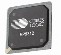
EP9312-CBZ Cirrus Logic Inc, EP9312-CBZ Datasheet - Page 276

EP9312-CBZ
Manufacturer Part Number
EP9312-CBZ
Description
IC ARM9 SOC UNIVERSAL 352PBGA
Manufacturer
Cirrus Logic Inc
Series
EP9r
Specifications of EP9312-CBZ
Core Size
16/32-Bit
Core Processor
ARM9
Speed
200MHz
Connectivity
EBI/EMI, EIDE, Ethernet, I²C, IrDA, Keypad/Touchscreen, SPI, UART/USART, USB
Peripherals
AC'97, DMA, I²:S, LCD, LED, MaverickKey, POR, PWM, WDT
Number Of I /o
16
Program Memory Type
ROMless
Ram Size
32K x 8
Voltage - Supply (vcc/vdd)
1.65 V ~ 3.6 V
Data Converters
A/D 8x12b
Oscillator Type
External
Operating Temperature
0°C ~ 70°C
Package / Case
352-BGA
Controller Family/series
(ARM9)
No. Of I/o's
16
Ram Memory Size
16MB
Cpu Speed
200MHz
No. Of Timers
4
No. Of Pwm Channels
2
Digital Ic Case Style
BGA
Embedded Interface Type
AC97, I2S, SPI, UART, USB
Rohs Compliant
Yes
Processor Series
EP93xx
Core
ARM920T
Data Bus Width
32 bit
3rd Party Development Tools
MDK-ARM, RL-ARM, ULINK2
Lead Free Status / RoHS Status
Lead free / RoHS Compliant
Eeprom Size
-
Program Memory Size
-
Lead Free Status / Rohs Status
Details
Other names
598-1258
Available stocks
Company
Part Number
Manufacturer
Quantity
Price
- Current page: 276 of 824
- Download datasheet (13Mb)
8
8-12
Graphics Accelerator
EP93xx User’s Guide
8.5.2.4 24 BPP mode
Let the starting SDRAM address of the destination image be 0x0044.
Pixel 0 starts at bit 16. The start pixel, P0, is in the word at address 0x0044 and has a
beginning bit position of 16. This makes 16 = 0x10 the value that is used for the SPEL field in
the
The end pixel, P7, is in the word at address 0x0054 and has a beginning bit position of 0. This
makes 0 = 0x0 the value that is used for the EPEL field in the
This 24 BPP mode is the most difficult because, unlike the other modes, pixels will span
words. For a Block Copy where 6 pixels are transferred per scan line, let the starting SDRAM
address of the source image be 0x0000.
start pixel, P1, is in the word at address 0x0000 and has a beginning bit position of 24. This
makes 24 = 0x18 the value that is used for the SPEL field in the
Let the starting SDRAM address of the destination image be 0x0058.
Pixel 1 starts at bit 24. The start pixel, P1, is in the word at address 0x0058 and has a
beginning bit position of 24. This makes 24 = 0x18 the value that is used for the SPEL field in
the
The end pixel, P6, is in the word at address 0x006C and has a beginning bit position of 0.
This makes 0 = 0x0 the value that is used for the EPEL field in the
register.
Note:The word count for this example would be: 5 - 1 = 4 words, since P7 ends in the 5th word.
“DESTPIXELSTRT”
“DESTPIXELSTRT”
Address
Address
0x004C
0x000C
0x0044
0x0048
0x0050
0x0054
0x0000
0x0004
0x0008
0x0010
0x0014
So, WIDTH = 0x4 would be written to the
31
31
Table 8-18. 16 BPP Memory Layout for Destination Image
Table 8-19. 24 BPP Memory Layout for Source Image
P1
P2
P3
P5
P6
P7
register.
register.
24 23
P0
P2
P4
P6
Copyright 2007 Cirrus Logic
P0
P2
P3
P4
P6
P7
Table 8-19
“BLKDESTWIDTH”
16 15
16 15
shows that Pixel 1 starts at bit 24. The
P0
P1
P3
P4
P5
P7
“DESTPIXELSTRT”
register.
8 7
P1
P3
P5
P7
“SRCPIXELSTRT”
“DESTPIXELSTRT”
Table 8-18
Table 8-20
P0
P1
P2
P4
P5
P6
0
0
shows that
shows that
register.
DS785UM1
register.
Related parts for EP9312-CBZ
Image
Part Number
Description
Manufacturer
Datasheet
Request
R

Part Number:
Description:
IC ARM920T MCU 200MHZ 352-PBGA
Manufacturer:
Cirrus Logic Inc
Datasheet:

Part Number:
Description:
System-on-Chip Processor
Manufacturer:
Cirrus Logic Inc
Datasheet:

Part Number:
Description:
IC ARM920T MCU 200MHZ 352-PBGA
Manufacturer:
Cirrus Logic Inc
Datasheet:

Part Number:
Description:
Development Kit
Manufacturer:
Cirrus Logic Inc
Datasheet:

Part Number:
Description:
Development Kit
Manufacturer:
Cirrus Logic Inc
Datasheet:

Part Number:
Description:
High-efficiency PFC + Fluorescent Lamp Driver Reference Design
Manufacturer:
Cirrus Logic Inc
Datasheet:

Part Number:
Description:
Development Kit
Manufacturer:
Cirrus Logic Inc
Datasheet:

Part Number:
Description:
Development Kit
Manufacturer:
Cirrus Logic Inc
Datasheet:

Part Number:
Description:
Development Kit
Manufacturer:
Cirrus Logic Inc
Datasheet:

Part Number:
Description:
Development Kit
Manufacturer:
Cirrus Logic Inc
Datasheet:

Part Number:
Description:
Development Kit
Manufacturer:
Cirrus Logic Inc
Datasheet:

Part Number:
Description:
Development Kit
Manufacturer:
Cirrus Logic Inc
Datasheet:

Part Number:
Description:
Ref Bd For Speakerbar MSA & DSP Products
Manufacturer:
Cirrus Logic Inc


