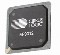
EP9312-CBZ Cirrus Logic Inc, EP9312-CBZ Datasheet - Page 504

EP9312-CBZ
Manufacturer Part Number
EP9312-CBZ
Description
IC ARM9 SOC UNIVERSAL 352PBGA
Manufacturer
Cirrus Logic Inc
Series
EP9r
Specifications of EP9312-CBZ
Core Size
16/32-Bit
Core Processor
ARM9
Speed
200MHz
Connectivity
EBI/EMI, EIDE, Ethernet, I²C, IrDA, Keypad/Touchscreen, SPI, UART/USART, USB
Peripherals
AC'97, DMA, I²:S, LCD, LED, MaverickKey, POR, PWM, WDT
Number Of I /o
16
Program Memory Type
ROMless
Ram Size
32K x 8
Voltage - Supply (vcc/vdd)
1.65 V ~ 3.6 V
Data Converters
A/D 8x12b
Oscillator Type
External
Operating Temperature
0°C ~ 70°C
Package / Case
352-BGA
Controller Family/series
(ARM9)
No. Of I/o's
16
Ram Memory Size
16MB
Cpu Speed
200MHz
No. Of Timers
4
No. Of Pwm Channels
2
Digital Ic Case Style
BGA
Embedded Interface Type
AC97, I2S, SPI, UART, USB
Rohs Compliant
Yes
Processor Series
EP93xx
Core
ARM920T
Data Bus Width
32 bit
3rd Party Development Tools
MDK-ARM, RL-ARM, ULINK2
Lead Free Status / RoHS Status
Lead free / RoHS Compliant
Eeprom Size
-
Program Memory Size
-
Lead Free Status / Rohs Status
Details
Other names
598-1258
Available stocks
Company
Part Number
Manufacturer
Quantity
Price
- Current page: 504 of 824
- Download datasheet (13Mb)
13
13-8
SDRAM, SyncROM, and SyncFLASH Controller
EP93xx User’s Guide
13.6.1 Entering Self Refresh Mode
13.6.2 Exiting Self Refresh Mode
13.6 SDRAM Self Refresh
13.7 Programming Registers: SyncFLASH Device
When using a 16-bit wide external memory bus, the following Read addresses must be used
to set up the specified parameters, where H can be 0, C, D, E or F as shown in
When entering the Standby mode, the following actions are carried out by the Synchronous
Memory controller before the processor is stopped:
When coming out of the Standby mode, the following actions are carried out by the
synchronous memory controller before the processor is started:
The programmable registers that are inside a SyncFLASH memory device, can be
programmed in a manner that is similar to programming the Mode register that is inside of an
SDRAM or SyncROM memory device.
The process of programming the SyncFLASH registers begins by writing WBM = ‘1’ to the
appropriate SDRAMDevCfg register to specify that burst-of-four reads and burst-of-one
writes will be used to access the device. Then, write LCR = ‘1’ to the GlConfig register. Doing
so causes the value of a subsequent read address to be used as the data value that is written
• SDRAM default READ Address: 0xH000_6600 — sets WBM=0, TM=0, CAS=3,
• SFLASH default READ Address: 0xH004_6600 — sets WBM=1, TM=0, CAS=3,
• SROM default READ Address: 0xH000_C400 — sets RAS=2, CAS=5, Sequential, BL=8
1. Issue Precharge accesses to all active banks
2. Issue NOP commands
3. SDCLKEN output driven low
4. Issue AUTO REFRESH command
5. Enter SELF REFRESH Mode
1. Allow clock stabilization
2. SDCLKEN output driven high
3. Issue ten NOP accesses
4. Issue AUTO REFRESH accesses
5. Exit SELF REFRESH Mode
Sequential, BL=8
Sequential, BL=8
Copyright 2007 Cirrus Logic
Table
DS785UM1
13-2:
Related parts for EP9312-CBZ
Image
Part Number
Description
Manufacturer
Datasheet
Request
R

Part Number:
Description:
IC ARM920T MCU 200MHZ 352-PBGA
Manufacturer:
Cirrus Logic Inc
Datasheet:

Part Number:
Description:
System-on-Chip Processor
Manufacturer:
Cirrus Logic Inc
Datasheet:

Part Number:
Description:
IC ARM920T MCU 200MHZ 352-PBGA
Manufacturer:
Cirrus Logic Inc
Datasheet:

Part Number:
Description:
Development Kit
Manufacturer:
Cirrus Logic Inc
Datasheet:

Part Number:
Description:
Development Kit
Manufacturer:
Cirrus Logic Inc
Datasheet:

Part Number:
Description:
High-efficiency PFC + Fluorescent Lamp Driver Reference Design
Manufacturer:
Cirrus Logic Inc
Datasheet:

Part Number:
Description:
Development Kit
Manufacturer:
Cirrus Logic Inc
Datasheet:

Part Number:
Description:
Development Kit
Manufacturer:
Cirrus Logic Inc
Datasheet:

Part Number:
Description:
Development Kit
Manufacturer:
Cirrus Logic Inc
Datasheet:

Part Number:
Description:
Development Kit
Manufacturer:
Cirrus Logic Inc
Datasheet:

Part Number:
Description:
Development Kit
Manufacturer:
Cirrus Logic Inc
Datasheet:

Part Number:
Description:
Development Kit
Manufacturer:
Cirrus Logic Inc
Datasheet:

Part Number:
Description:
Ref Bd For Speakerbar MSA & DSP Products
Manufacturer:
Cirrus Logic Inc


