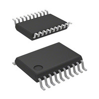
R5F21324ANSP#U1 Renesas Electronics America, R5F21324ANSP#U1 Datasheet - Page 199

R5F21324ANSP#U1
Manufacturer Part Number
R5F21324ANSP#U1
Description
MCU 1KB FLASH 16K ROM 20-LSSOP
Manufacturer
Renesas Electronics America
Series
R8C/3x/32Ar
Datasheet
1.R5F21322ANSPU1.pdf
(629 pages)
Specifications of R5F21324ANSP#U1
Core Processor
R8C
Core Size
16/32-Bit
Speed
20MHz
Connectivity
I²C, LIN, SIO, SSU, UART/USART
Peripherals
POR, PWM, Voltage Detect, WDT
Number Of I /o
15
Program Memory Size
16KB (16K x 8)
Program Memory Type
FLASH
Ram Size
1.5K x 8
Voltage - Supply (vcc/vdd)
1.8 V ~ 5.5 V
Data Converters
A/D 4x10b
Oscillator Type
Internal
Operating Temperature
-20°C ~ 85°C
Package / Case
20-LSSOP
Lead Free Status / RoHS Status
Lead free / RoHS Compliant
Eeprom Size
-
Available stocks
Company
Part Number
Manufacturer
Quantity
Price
- Current page: 199 of 629
- Download datasheet (7Mb)
Under development
R8C/32A Group
REJ09B0458-0020 Rev.0.20
Page 169 of 583
15.2.7
i = 0 to 3, 5, 6
Table 15.2
After Reset
DTCEN0
DTCEN1
DTCEN2
DTCEN3
DTCEN5
DTCEN6
Register
Bit
b0
b1
b2
b3
b4
b5
b6
b7
Address 0088h (DTCEN0), 0089h (DTCEN1), 008Ah (DTCEN2), 008Bh (DTCEN3),
The DTCENi registers enable/disable DTC activation by interrupt sources. Table 15.2 shows Correspondences
between Bits DTCENi0 to DTCENi1, DTCENi3 to DTCENi7 (i = 0 to 3, 5, 6) and Interrupt Sources.
Symbol DTCENi7 DTCENi6 DTCENi5 DTCENi4 DTCENi3
DTCENi0 DTC activation enable bit
DTCENi1
DTCENi3 DTC activation enable bit
DTCENi4
DTCENi5
DTCENi6
DTCENi7
Symbol
Bit
DTC Activation Enable Register i (DTCENi) (i = 0 to 3, 5, 6)
—
input-capture/
008Dh (DTCEN5), 008Eh (DTCEN6)
DTCENi7 Bit
SSU/I
receive data
Timer RC
compare-
Key input
3, 5, 6) and Interrupt Sources
Preliminary specification
Specifications in this manual are tentative and subject to change.
Correspondences between Bits DTCENi0 to DTCENi1, DTCENi3 to DTCENi7 (i = 0 to
match C
INT0
b7
0
full
—
—
2
Reserved bit
C bus
b6
input-capture/
transmit data
0
DTCENi6 Bit
SSU/I
conversion
Timer RC
compare-
Timer RA
Nov 05, 2008
match D
empty
INT1
Bit Name
A/D
—
2
C bus
b5
0
comparator A2
DTCENi5 Bit
monitor 2/
Timer RE
reception
Voltage
UART0
—
—
—
b4
0
0: Activation disabled
1: Activation enabled
Set to 0.
0: Activation disabled
1: Activation enabled
comparator A1
DTCENi4 Bit
transmission
monitor 1/
Timer RB
b3
0
Voltage
UART0
INT3
—
—
b2
—
0
DTCENi3 Bit
Flash ready
status
DTCENi1 DTCENi0
Function
—
—
—
—
—
b1
0
input-capture/
DTCENi1 Bit
Timer RC
compare-
reception
match A
UART2
b0
0
—
—
—
—
input-capture/
DTCENi0 Bit
transmission
Timer RC
compare-
match B
UART2
—
—
—
—
15. DTC
R/W
R/W
R/W
R/W
R/W
R/W
R/W
R/W
R/W
Related parts for R5F21324ANSP#U1
Image
Part Number
Description
Manufacturer
Datasheet
Request
R

Part Number:
Description:
KIT STARTER FOR M16C/29
Manufacturer:
Renesas Electronics America
Datasheet:

Part Number:
Description:
KIT STARTER FOR R8C/2D
Manufacturer:
Renesas Electronics America
Datasheet:

Part Number:
Description:
R0K33062P STARTER KIT
Manufacturer:
Renesas Electronics America
Datasheet:

Part Number:
Description:
KIT STARTER FOR R8C/23 E8A
Manufacturer:
Renesas Electronics America
Datasheet:

Part Number:
Description:
KIT STARTER FOR R8C/25
Manufacturer:
Renesas Electronics America
Datasheet:

Part Number:
Description:
KIT STARTER H8S2456 SHARPE DSPLY
Manufacturer:
Renesas Electronics America
Datasheet:

Part Number:
Description:
KIT STARTER FOR R8C38C
Manufacturer:
Renesas Electronics America
Datasheet:

Part Number:
Description:
KIT STARTER FOR R8C35C
Manufacturer:
Renesas Electronics America
Datasheet:

Part Number:
Description:
KIT STARTER FOR R8CL3AC+LCD APPS
Manufacturer:
Renesas Electronics America
Datasheet:

Part Number:
Description:
KIT STARTER FOR RX610
Manufacturer:
Renesas Electronics America
Datasheet:

Part Number:
Description:
KIT STARTER FOR R32C/118
Manufacturer:
Renesas Electronics America
Datasheet:

Part Number:
Description:
KIT DEV RSK-R8C/26-29
Manufacturer:
Renesas Electronics America
Datasheet:

Part Number:
Description:
KIT STARTER FOR SH7124
Manufacturer:
Renesas Electronics America
Datasheet:

Part Number:
Description:
KIT STARTER FOR H8SX/1622
Manufacturer:
Renesas Electronics America
Datasheet:

Part Number:
Description:
KIT DEV FOR SH7203
Manufacturer:
Renesas Electronics America
Datasheet:


