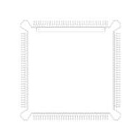
MC68HC16Z1CEH16 Freescale Semiconductor, MC68HC16Z1CEH16 Datasheet - Page 200

MC68HC16Z1CEH16
Manufacturer Part Number
MC68HC16Z1CEH16
Description
IC MCU 16BIT 16MHZ 132-PQFP
Manufacturer
Freescale Semiconductor
Series
HC16r
Specifications of MC68HC16Z1CEH16
Core Processor
CPU16
Core Size
16-Bit
Speed
16MHz
Connectivity
EBI/EMI, SCI, SPI
Peripherals
POR, PWM, WDT
Number Of I /o
16
Program Memory Type
ROMless
Ram Size
1K x 8
Voltage - Supply (vcc/vdd)
2.7 V ~ 5.5 V
Data Converters
A/D 8x10b
Oscillator Type
Internal
Operating Temperature
-40°C ~ 85°C
Package / Case
132-QFP
Processor Series
HC16Z
Core
CPU16
Data Bus Width
16 bit
Controller Family/series
68HC16
No. Of I/o's
26
Ram Memory Size
1KB
Cpu Speed
16MHz
No. Of Timers
2
Embedded Interface Type
QSPI, SCI
Rohs Compliant
Yes
Package
132PQFP
Family Name
HC16
Maximum Speed
16 MHz
Operating Supply Voltage
3.3|5 V
Number Of Programmable I/os
16
On-chip Adc
8-chx10-bit
Number Of Timers
11
Data Ram Size
1 KB
Interface Type
SCI, SPI, UART
Maximum Clock Frequency
16 MHz
Maximum Operating Temperature
+ 85 C
Mounting Style
SMD/SMT
Minimum Operating Temperature
- 40 C
Lead Free Status / RoHS Status
Lead free / RoHS Compliant
Eeprom Size
-
Program Memory Size
-
Lead Free Status / Rohs Status
Lead free / RoHS Compliant
Available stocks
Company
Part Number
Manufacturer
Quantity
Price
Company:
Part Number:
MC68HC16Z1CEH16
Manufacturer:
Freescale Semiconductor
Quantity:
10 000
Part Number:
MC68HC16Z1CEH16
Manufacturer:
FREESCALE
Quantity:
20 000
- Current page: 200 of 500
- Download datasheet (6Mb)
8.8 Pin Considerations
8.8.1 Analog Reference Pins
8.8.2 Analog Power Pins
8-14
Result Data Format
right-justified format
Refer to
The ADC requires accurate, noise-free input signals for proper operation. The follow-
ing sections discuss the design of external circuitry to maximize ADC performance.
No A/D converter can be more accurate than its analog reference. Any noise in the
reference can result in at least that much error in a conversion. The reference for the
ADC, supplied by pins V
tain a noise-free, clean signal. In many cases, simple capacitive bypassing may suf-
fice. In extreme cases, inductors or ferrite beads may be necessary if noise or RF
energy is present. Series resistance is not advisable since there is an effective DC cur-
rent requirement from the reference voltage by the internal resistor string in the RC
DAC array. External resistance may introduce error in this architecture under certain
conditions. Any series devices in the filter network should contain a minimum amount
of DC resistance.
For accurate conversion results, the analog reference voltages must be within the lim-
its defined by V
The analog supply pins (V
ages (V
the analog input circuitry.
left-justified format
left-justified format
Unsigned
Unsigned
Signed
RH
APPENDIX D REGISTER SUMMARY
and V
DDA
RL
Conversion result is unsigned right-justified data. Bits [9:0] are used for 10-bit resolution,
bits [7:0] are used for 8-bit conversion (bits [9:8] are zero). Bits [15:10] always return zero
when read.
Conversion result is signed left-justified data. Bits [15:6] are used for 10-bit resolution, bits
[15:8] are used for 8-bit conversion (bits [7:6] are zero). Although the ADC is unipolar, it
is assumed that the zero point is (V RH – V RL ) / 2 when this format is used. The value read
from the register is an offset two’s-complement number; for positive input, bit 15 equals
zero, for negative input, bit 15 equals one. Bits [5:0] always return zero when read.
Conversion result is unsigned left-justified data. Bits [15:6] are used for 10-bit resolution,
bits [15:8] are used for 8-bit conversion (bits [7:6] are zero). Bits [5:0] always return zero
when read.
) and of the analog multiplexer inputs.
Freescale Semiconductor, Inc.
and V
For More Information On This Product,
Table 8-9 Result Register Formats
RH
ANALOG-TO-DIGITAL CONVERTER
DDA
SSA
and V
Go to: www.freescale.com
, as explained in the following subsection.
and V
RL
, should be low-pass filtered from its source to ob-
SSA
) define the limits of the analog reference volt-
Description
for register mapping and configuration.
Figure 8-4
M68HC16 Z SERIES
USER’S MANUAL
is a diagram of
Related parts for MC68HC16Z1CEH16
Image
Part Number
Description
Manufacturer
Datasheet
Request
R
Part Number:
Description:
Manufacturer:
Freescale Semiconductor, Inc
Datasheet:
Part Number:
Description:
Manufacturer:
Freescale Semiconductor, Inc
Datasheet:
Part Number:
Description:
Manufacturer:
Freescale Semiconductor, Inc
Datasheet:
Part Number:
Description:
Manufacturer:
Freescale Semiconductor, Inc
Datasheet:
Part Number:
Description:
Manufacturer:
Freescale Semiconductor, Inc
Datasheet:
Part Number:
Description:
Manufacturer:
Freescale Semiconductor, Inc
Datasheet:
Part Number:
Description:
Manufacturer:
Freescale Semiconductor, Inc
Datasheet:
Part Number:
Description:
Manufacturer:
Freescale Semiconductor, Inc
Datasheet:
Part Number:
Description:
Manufacturer:
Freescale Semiconductor, Inc
Datasheet:
Part Number:
Description:
Manufacturer:
Freescale Semiconductor, Inc
Datasheet:
Part Number:
Description:
Manufacturer:
Freescale Semiconductor, Inc
Datasheet:
Part Number:
Description:
Manufacturer:
Freescale Semiconductor, Inc
Datasheet:
Part Number:
Description:
Manufacturer:
Freescale Semiconductor, Inc
Datasheet:
Part Number:
Description:
Manufacturer:
Freescale Semiconductor, Inc
Datasheet:
Part Number:
Description:
Manufacturer:
Freescale Semiconductor, Inc
Datasheet:


