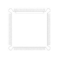
MC68HC16Z1CEH16 Freescale Semiconductor, MC68HC16Z1CEH16 Datasheet - Page 237

MC68HC16Z1CEH16
Manufacturer Part Number
MC68HC16Z1CEH16
Description
IC MCU 16BIT 16MHZ 132-PQFP
Manufacturer
Freescale Semiconductor
Series
HC16r
Specifications of MC68HC16Z1CEH16
Core Processor
CPU16
Core Size
16-Bit
Speed
16MHz
Connectivity
EBI/EMI, SCI, SPI
Peripherals
POR, PWM, WDT
Number Of I /o
16
Program Memory Type
ROMless
Ram Size
1K x 8
Voltage - Supply (vcc/vdd)
2.7 V ~ 5.5 V
Data Converters
A/D 8x10b
Oscillator Type
Internal
Operating Temperature
-40°C ~ 85°C
Package / Case
132-QFP
Processor Series
HC16Z
Core
CPU16
Data Bus Width
16 bit
Controller Family/series
68HC16
No. Of I/o's
26
Ram Memory Size
1KB
Cpu Speed
16MHz
No. Of Timers
2
Embedded Interface Type
QSPI, SCI
Rohs Compliant
Yes
Package
132PQFP
Family Name
HC16
Maximum Speed
16 MHz
Operating Supply Voltage
3.3|5 V
Number Of Programmable I/os
16
On-chip Adc
8-chx10-bit
Number Of Timers
11
Data Ram Size
1 KB
Interface Type
SCI, SPI, UART
Maximum Clock Frequency
16 MHz
Maximum Operating Temperature
+ 85 C
Mounting Style
SMD/SMT
Minimum Operating Temperature
- 40 C
Lead Free Status / RoHS Status
Lead free / RoHS Compliant
Eeprom Size
-
Program Memory Size
-
Lead Free Status / Rohs Status
Lead free / RoHS Compliant
Available stocks
Company
Part Number
Manufacturer
Quantity
Price
Company:
Part Number:
MC68HC16Z1CEH16
Manufacturer:
Freescale Semiconductor
Quantity:
10 000
Part Number:
MC68HC16Z1CEH16
Manufacturer:
FREESCALE
Quantity:
20 000
- Current page: 237 of 500
- Download datasheet (6Mb)
9.4.3.5 Transmitter Operation
M68HC16 Z SERIES
USER’S MANUAL
The transmitter consists of a serial shifter and a parallel data register (TDR) located in
the SCI data register (SCDR). The serial shifter cannot be directly accessed by the
CPU16. The transmitter is double-buffered, which means that data can be loaded into
TDR while other data is shifted out. The TE bit in SCCR1 enables (TE = 1) and dis-
ables (TE = 0) the transmitter.
The shifter output is connected to the TXD pin while the transmitter is operating (TE =
1, or TE = 0 and transmission in progress). Wired-OR operation should be specified
when more than one transmitter is used on the same SCI bus. The WOMS bit in
SCCR1 determines whether TXD is an open-drain (wired-OR) output or a normal
CMOS output. An external pull-up resistor on TXD is necessary for wired-OR opera-
tion. WOMS controls TXD function whether the pin is used by the SCI or as a general-
purpose I/O pin.
Data to be transmitted is written to SCDR, then transferred to the serial shifter. The
transmit data register empty (TDRE) flag in SCSR shows the status of TDR. When
TDRE = 0, TDR contains data that has not been transferred to the shifter. Writing to
SCDR again overwrites the data. TDRE is set when the data in TDR is transferred to
the shifter. Before new data can be written to SCDR, however, the processor must
clear TDRE by writing to SCSR. If new data is written to SCDR without first clearing
TDRE, the data will not be transmitted.
The transmission complete (TC) flag in SCSR shows transmitter shifter state. When
TC = 0, the shifter is busy. TC is set when all shifting operations are completed. TC is
not automatically cleared. The processor must clear it by first reading SCSR while TC
is set, then writing new data to SCDR.
The state of the serial shifter is checked when the TE bit is set. If TC = 1, an idle frame
is transmitted as a preamble to the following data frame. If TC = 0, the current opera-
tion continues until the final bit in the frame is sent, then the preamble is transmitted.
The TC bit is set at the end of preamble transmission.
The SBK bit in SCCR1 is used to insert break frames in a transmission. A non-zero
integer number of break frames is transmitted while SBK is set. Break transmission
begins when SBK is set, and ends with the transmission in progress at the time either
SBK or TE is cleared. If SBK is set while a transmission is in progress, that transmis-
sion finishes normally before the break begins. To assure the minimum break time,
toggle SBK quickly to one and back to zero. The TC bit is set at the end of break trans-
mission. After break transmission, at least one bit-time of logic level one (mark idle) is
transmitted to ensure that a subsequent start bit can be detected.
Table 9-5 Effect of Parity Checking on Data Size
Freescale Semiconductor, Inc.
M
0
0
1
1
For More Information On This Product,
QUEUED SERIAL MODULE
Go to: www.freescale.com
PE
0
1
0
1
8 data bits
7 data bits, 1 parity bit
9 data bits
8 data bits, 1 parity bit
Result
9-27
Related parts for MC68HC16Z1CEH16
Image
Part Number
Description
Manufacturer
Datasheet
Request
R
Part Number:
Description:
Manufacturer:
Freescale Semiconductor, Inc
Datasheet:
Part Number:
Description:
Manufacturer:
Freescale Semiconductor, Inc
Datasheet:
Part Number:
Description:
Manufacturer:
Freescale Semiconductor, Inc
Datasheet:
Part Number:
Description:
Manufacturer:
Freescale Semiconductor, Inc
Datasheet:
Part Number:
Description:
Manufacturer:
Freescale Semiconductor, Inc
Datasheet:
Part Number:
Description:
Manufacturer:
Freescale Semiconductor, Inc
Datasheet:
Part Number:
Description:
Manufacturer:
Freescale Semiconductor, Inc
Datasheet:
Part Number:
Description:
Manufacturer:
Freescale Semiconductor, Inc
Datasheet:
Part Number:
Description:
Manufacturer:
Freescale Semiconductor, Inc
Datasheet:
Part Number:
Description:
Manufacturer:
Freescale Semiconductor, Inc
Datasheet:
Part Number:
Description:
Manufacturer:
Freescale Semiconductor, Inc
Datasheet:
Part Number:
Description:
Manufacturer:
Freescale Semiconductor, Inc
Datasheet:
Part Number:
Description:
Manufacturer:
Freescale Semiconductor, Inc
Datasheet:
Part Number:
Description:
Manufacturer:
Freescale Semiconductor, Inc
Datasheet:
Part Number:
Description:
Manufacturer:
Freescale Semiconductor, Inc
Datasheet:


