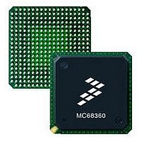
MC68EN360CAI25L Freescale Semiconductor, MC68EN360CAI25L Datasheet - Page 104

MC68EN360CAI25L
Manufacturer Part Number
MC68EN360CAI25L
Description
IC MPU QUICC 25MHZ 240-FQFP
Manufacturer
Freescale Semiconductor
Series
MC68000r
Datasheets
1.MC68EN302AG20BT.pdf
(8 pages)
2.MC68EN360VR25L.pdf
(14 pages)
3.MC68EN360VR25L.pdf
(2 pages)
4.MC68EN360CAI25L.pdf
(962 pages)
Specifications of MC68EN360CAI25L
Processor Type
M683xx 32-Bit
Speed
25MHz
Voltage
5V
Mounting Type
Surface Mount
Package / Case
240-FQFP
Core Size
32 Bit
Cpu Speed
25MHz
Embedded Interface Type
SCP, TDM
Digital Ic Case Style
FQFP
No. Of Pins
240
Supply Voltage Range
4.75V To 5.25V
Rohs Compliant
Yes
Family Name
M68xxx
Device Core
ColdFire
Device Core Size
32b
Frequency (max)
25MHz
Instruction Set Architecture
RISC
Supply Voltage 1 (typ)
5V
Operating Supply Voltage (max)
5.25V
Operating Supply Voltage (min)
4.75V
Operating Temp Range
-40C to 85C
Operating Temperature Classification
Industrial
Mounting
Surface Mount
Pin Count
240
Package Type
FQFP
Lead Free Status / RoHS Status
Lead free / RoHS Compliant
Features
-
Lead Free Status / Rohs Status
Compliant
Available stocks
Company
Part Number
Manufacturer
Quantity
Price
Company:
Part Number:
MC68EN360CAI25L
Manufacturer:
APLHA
Quantity:
12 000
Company:
Part Number:
MC68EN360CAI25L
Manufacturer:
Freescale Semiconductor
Quantity:
10 000
Part Number:
MC68EN360CAI25L
Manufacturer:
FREESCALE
Quantity:
20 000
- MC68EN302AG20BT PDF datasheet
- MC68EN360VR25L PDF datasheet #2
- MC68EN360VR25L PDF datasheet #3
- MC68EN360CAI25L PDF datasheet #4
- Current page: 104 of 962
- Download datasheet (4Mb)
Freescale Semiconductor, Inc.
Bus Operation
State 3—The QUICC asserts DS during S3, indicating that data is stable on the data bus.
As long as at least one of the DSACKx signals is recognized by the end of S2 (meeting the
asynchronous input setup time requirement), the cycle terminates one clock later. If
DSACKx is not recognized by the start of S3, the QUICC inserts wait states instead of pro-
ceeding to S4 and S5. To ensure that wait states are inserted, both DSACK1 and DSACK0
must remain negated throughout the asynchronous input setup and hold times around the
end of S2. If wait states are added, the QUICC continues to sample DSACKx on the falling
edges of the clock until one is recognized. The selected device uses the four write enables
lines or R/W, SIZ1, SIZ0, A1, and A0 to latch data from the appropriate byte(s) of the data
bus (D31–D24, D23–D16, D15–D8, and D7–D0). WE3–WE0 or SIZ1, SIZ0, A1, and A0
select the bytes of the data bus. If it has not already done so, the device asserts DSACKx
to signal that it has successfully stored the data.
State 4—The QUICC issues no new control signals during S4.
State 5—The QUICC negates WE3–WE0, AS, and DS during S5. It holds the address and
data valid during S5 to provide address hold time for memory systems. R/W, SIZ1, SIZ0,
and FC3–FC0 also remain valid throughout S5. The external device must keep DSACKx
asserted until it detects the negation of AS or DS (whichever it detects first). The device must
negate DSACKx within approximately one clock period after sensing the negation of AS or
DS. DSACKx signals that remain asserted beyond this limit may be prematurely detected
for the next bus cycle.
4.3.3 Read-Modify-Write Cycle
The read-modify-write cycle performs a read, conditionally modifies the data in the arith-
metic logic unit, and may write the data out to memory. In the QUICC, this operation is indi-
visible, providing semaphore capabilities for multiprocessor systems. During the entire read-
modify-write sequence, the QUICC asserts RMC to indicate that an indivisible operation is
occurring. The QUICC does not issue a bus grant (BG) signal in response to a bus request
(BR) signal during this operation. Figure 4-21 is an example of a functional timing diagram
of a read-modify-write instruction specified in terms of clock periods.
4-28
MC68360 USER’S MANUAL
For More Information On This Product,
Go to: www.freescale.com
Related parts for MC68EN360CAI25L
Image
Part Number
Description
Manufacturer
Datasheet
Request
R
Part Number:
Description:
Manufacturer:
Freescale Semiconductor, Inc
Datasheet:
Part Number:
Description:
Manufacturer:
Freescale Semiconductor, Inc
Datasheet:
Part Number:
Description:
Manufacturer:
Freescale Semiconductor, Inc
Datasheet:
Part Number:
Description:
Manufacturer:
Freescale Semiconductor, Inc
Datasheet:
Part Number:
Description:
Manufacturer:
Freescale Semiconductor, Inc
Datasheet:
Part Number:
Description:
Manufacturer:
Freescale Semiconductor, Inc
Datasheet:
Part Number:
Description:
Manufacturer:
Freescale Semiconductor, Inc
Datasheet:
Part Number:
Description:
Manufacturer:
Freescale Semiconductor, Inc
Datasheet:
Part Number:
Description:
Manufacturer:
Freescale Semiconductor, Inc
Datasheet:
Part Number:
Description:
Manufacturer:
Freescale Semiconductor, Inc
Datasheet:
Part Number:
Description:
Manufacturer:
Freescale Semiconductor, Inc
Datasheet:
Part Number:
Description:
Manufacturer:
Freescale Semiconductor, Inc
Datasheet:
Part Number:
Description:
Manufacturer:
Freescale Semiconductor, Inc
Datasheet:
Part Number:
Description:
Manufacturer:
Freescale Semiconductor, Inc
Datasheet:
Part Number:
Description:
Manufacturer:
Freescale Semiconductor, Inc
Datasheet:


