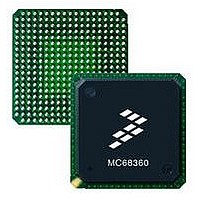
MC68EN360CAI25L Freescale Semiconductor, MC68EN360CAI25L Datasheet - Page 49

MC68EN360CAI25L
Manufacturer Part Number
MC68EN360CAI25L
Description
IC MPU QUICC 25MHZ 240-FQFP
Manufacturer
Freescale Semiconductor
Series
MC68000r
Datasheets
1.MC68EN302AG20BT.pdf
(8 pages)
2.MC68EN360VR25L.pdf
(14 pages)
3.MC68EN360VR25L.pdf
(2 pages)
4.MC68EN360CAI25L.pdf
(962 pages)
Specifications of MC68EN360CAI25L
Processor Type
M683xx 32-Bit
Speed
25MHz
Voltage
5V
Mounting Type
Surface Mount
Package / Case
240-FQFP
Core Size
32 Bit
Cpu Speed
25MHz
Embedded Interface Type
SCP, TDM
Digital Ic Case Style
FQFP
No. Of Pins
240
Supply Voltage Range
4.75V To 5.25V
Rohs Compliant
Yes
Family Name
M68xxx
Device Core
ColdFire
Device Core Size
32b
Frequency (max)
25MHz
Instruction Set Architecture
RISC
Supply Voltage 1 (typ)
5V
Operating Supply Voltage (max)
5.25V
Operating Supply Voltage (min)
4.75V
Operating Temp Range
-40C to 85C
Operating Temperature Classification
Industrial
Mounting
Surface Mount
Pin Count
240
Package Type
FQFP
Lead Free Status / RoHS Status
Lead free / RoHS Compliant
Features
-
Lead Free Status / Rohs Status
Compliant
Available stocks
Company
Part Number
Manufacturer
Quantity
Price
Company:
Part Number:
MC68EN360CAI25L
Manufacturer:
APLHA
Quantity:
12 000
Company:
Part Number:
MC68EN360CAI25L
Manufacturer:
Freescale Semiconductor
Quantity:
10 000
Part Number:
MC68EN360CAI25L
Manufacturer:
FREESCALE
Quantity:
20 000
- MC68EN302AG20BT PDF datasheet
- MC68EN360VR25L PDF datasheet #2
- MC68EN360VR25L PDF datasheet #3
- MC68EN360CAI25L PDF datasheet #4
- Current page: 49 of 962
- Download datasheet (4Mb)
SECTION 2
SIGNAL DESCRIPTIONS
This section contains brief descriptions of the QUICC input and output signals in their func-
tional groups as shown in Figure 2-1.
2.1 SYSTEM BUS SIGNAL INDEX
The QUICC system bus signals consist of two groups. The first group, listed in Table 2-1,
consists of system bus signals that exist when the QUICC is in the normal mode (CPU32+
enabled). The second group consists of system bus signals that exist when the QUICC is in
the slave mode (CPU32+ disabled). They are listed in Table 2-7 and may also be identified
in Figure 2-1 as those with an italic font. In Table 2-1, the signal name, mnemonic, and a
brief functional description are presented. For more detail on each signal, refer to the para-
graphs that discuss each signal.
2.1.1 Address Bus
The address bus consists of the following two groups. Refer to Section 4 Bus Operation for
information on the address bus and its relationship to bus operation.
2.1.1.1 ADDRESS BUS (A27–A0). This three-state bidirectional bus (along with A31–A28)
provides the address for the current bus cycle, except in the CPU address space. Refer to
Section 4 Bus Operation for more information on the CPU address space. A27 is the most
significant address signal in this group.
2.1.1.2 ADDRESS BUS (A31–A28). These pins can be programmed as the most signifi-
cant four address bits or as four byte write enables.
A31–A28—These pins can function as the most significant 4 address bits. A31 is the
most significant address signal in this group.
WE3–WE0—On a write cycle, these active-low signals indicates which byte of the 32-
bit data bus contains valid data.
WE0—Corresponds to A31 and selects data bits 31–24. Also may be referred to as UU-
WE.
WE1—Corresponds to A30 and selects data bits 23–16. Also may be referred to as UM-
WE.
WE2—Corresponds to A29 and selects data bits 15–8. Also may be referred to as LMWE.
WE3—Corresponds to A28 and selects data bits 7–0. Also may be referred to as LLWE.
Freescale Semiconductor, Inc.
Thi d
For More Information On This Product,
MC68360 USER’S MANUAL
Go to: www.freescale.com
t
t d ith F
M k 4 0 4
Related parts for MC68EN360CAI25L
Image
Part Number
Description
Manufacturer
Datasheet
Request
R
Part Number:
Description:
Manufacturer:
Freescale Semiconductor, Inc
Datasheet:
Part Number:
Description:
Manufacturer:
Freescale Semiconductor, Inc
Datasheet:
Part Number:
Description:
Manufacturer:
Freescale Semiconductor, Inc
Datasheet:
Part Number:
Description:
Manufacturer:
Freescale Semiconductor, Inc
Datasheet:
Part Number:
Description:
Manufacturer:
Freescale Semiconductor, Inc
Datasheet:
Part Number:
Description:
Manufacturer:
Freescale Semiconductor, Inc
Datasheet:
Part Number:
Description:
Manufacturer:
Freescale Semiconductor, Inc
Datasheet:
Part Number:
Description:
Manufacturer:
Freescale Semiconductor, Inc
Datasheet:
Part Number:
Description:
Manufacturer:
Freescale Semiconductor, Inc
Datasheet:
Part Number:
Description:
Manufacturer:
Freescale Semiconductor, Inc
Datasheet:
Part Number:
Description:
Manufacturer:
Freescale Semiconductor, Inc
Datasheet:
Part Number:
Description:
Manufacturer:
Freescale Semiconductor, Inc
Datasheet:
Part Number:
Description:
Manufacturer:
Freescale Semiconductor, Inc
Datasheet:
Part Number:
Description:
Manufacturer:
Freescale Semiconductor, Inc
Datasheet:
Part Number:
Description:
Manufacturer:
Freescale Semiconductor, Inc
Datasheet:


