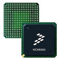
MC68EN360CAI25L Freescale Semiconductor, MC68EN360CAI25L Datasheet - Page 658

MC68EN360CAI25L
Manufacturer Part Number
MC68EN360CAI25L
Description
IC MPU QUICC 25MHZ 240-FQFP
Manufacturer
Freescale Semiconductor
Series
MC68000r
Datasheets
1.MC68EN302AG20BT.pdf
(8 pages)
2.MC68EN360VR25L.pdf
(14 pages)
3.MC68EN360VR25L.pdf
(2 pages)
4.MC68EN360CAI25L.pdf
(962 pages)
Specifications of MC68EN360CAI25L
Processor Type
M683xx 32-Bit
Speed
25MHz
Voltage
5V
Mounting Type
Surface Mount
Package / Case
240-FQFP
Core Size
32 Bit
Cpu Speed
25MHz
Embedded Interface Type
SCP, TDM
Digital Ic Case Style
FQFP
No. Of Pins
240
Supply Voltage Range
4.75V To 5.25V
Rohs Compliant
Yes
Family Name
M68xxx
Device Core
ColdFire
Device Core Size
32b
Frequency (max)
25MHz
Instruction Set Architecture
RISC
Supply Voltage 1 (typ)
5V
Operating Supply Voltage (max)
5.25V
Operating Supply Voltage (min)
4.75V
Operating Temp Range
-40C to 85C
Operating Temperature Classification
Industrial
Mounting
Surface Mount
Pin Count
240
Package Type
FQFP
Lead Free Status / RoHS Status
Lead free / RoHS Compliant
Features
-
Lead Free Status / Rohs Status
Compliant
Available stocks
Company
Part Number
Manufacturer
Quantity
Price
Company:
Part Number:
MC68EN360CAI25L
Manufacturer:
APLHA
Quantity:
12 000
Company:
Part Number:
MC68EN360CAI25L
Manufacturer:
Freescale Semiconductor
Quantity:
10 000
Part Number:
MC68EN360CAI25L
Manufacturer:
FREESCALE
Quantity:
20 000
- MC68EN302AG20BT PDF datasheet
- MC68EN360VR25L PDF datasheet #2
- MC68EN360VR25L PDF datasheet #3
- MC68EN360CAI25L PDF datasheet #4
- Current page: 658 of 962
- Download datasheet (4Mb)
Parallel Interface Port (PIP)
Thus, to connect to QUICCs using this interface, connect the STBO pin of each QUICC to
the STBI pin of the other and connect the desired data pins (either PB8–PB15 or PB0–PB15
are connected between QUICCs).
7.13.5 Pulsed Data Transfers
In the pulsed handshake mode, the PIP may be configured as a transmitter or a receiver.
This configuration allows a Centronics-compatible interface to be implemented.
The pulsed handshake mode may be controlled by the RISC or the CPU32+ core. Operation
using the RISC requires BDs and parameter RAM initialization very similar to the other serial
channels. Data is then stored in the buffers using one of the SDMA channels (one of the
available channels from SMC2). Operation by the CPU32+ core is performed by software-
controlled reads and writes from/to the PIP data register upon interrupt request.
When configured as a transmitter, the STBO pin (PB16) is used as a strobe output (STB)
handshake control signal, and the STBI pin (PB17) is used as an acknowledge (ACK) input.
When configured as a receiver, the PIP generates the ACK signal on the STBO pin and
inputs the STB signal on the STBI pin.
Bits PB16 and PB17 in the port B data direction register (PBDIR) and the port B data register
(PBDAT) corresponding to STBO and STBI are not valid and are ignored by the PIP when
the pulsed handshake mode is selected.
7-334
(OUTPUT READY)
(INPUT READY)
TRANSMITTER
TRANSMITTER
RECEIVER
DATA
ACK
STB
At the time of writing, RISC operation of the PIP has not been
fully defined. The user should use the CPU32+ core operation
mode until as RISC microcode becomes available or the full PIP
microcode is available in the RISC internal ROM. Please contact
the local Motorola sales representative to obtain the current sta-
tus of the PIP RISC microcode. In the following description, the
RISC reads and writes of the data register are replaced by
CPU32+ core reads and writes.
Figure 7-85. Interlock Handshake Mode
Freescale Semiconductor, Inc.
For More Information On This Product,
MC68360 USER’S MANUAL
T SETUP
Go to: www.freescale.com
NOTE
T HOLD
Related parts for MC68EN360CAI25L
Image
Part Number
Description
Manufacturer
Datasheet
Request
R
Part Number:
Description:
Manufacturer:
Freescale Semiconductor, Inc
Datasheet:
Part Number:
Description:
Manufacturer:
Freescale Semiconductor, Inc
Datasheet:
Part Number:
Description:
Manufacturer:
Freescale Semiconductor, Inc
Datasheet:
Part Number:
Description:
Manufacturer:
Freescale Semiconductor, Inc
Datasheet:
Part Number:
Description:
Manufacturer:
Freescale Semiconductor, Inc
Datasheet:
Part Number:
Description:
Manufacturer:
Freescale Semiconductor, Inc
Datasheet:
Part Number:
Description:
Manufacturer:
Freescale Semiconductor, Inc
Datasheet:
Part Number:
Description:
Manufacturer:
Freescale Semiconductor, Inc
Datasheet:
Part Number:
Description:
Manufacturer:
Freescale Semiconductor, Inc
Datasheet:
Part Number:
Description:
Manufacturer:
Freescale Semiconductor, Inc
Datasheet:
Part Number:
Description:
Manufacturer:
Freescale Semiconductor, Inc
Datasheet:
Part Number:
Description:
Manufacturer:
Freescale Semiconductor, Inc
Datasheet:
Part Number:
Description:
Manufacturer:
Freescale Semiconductor, Inc
Datasheet:
Part Number:
Description:
Manufacturer:
Freescale Semiconductor, Inc
Datasheet:
Part Number:
Description:
Manufacturer:
Freescale Semiconductor, Inc
Datasheet:


