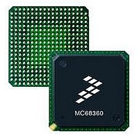
MC68EN360CAI25L Freescale Semiconductor, MC68EN360CAI25L Datasheet - Page 303

MC68EN360CAI25L
Manufacturer Part Number
MC68EN360CAI25L
Description
IC MPU QUICC 25MHZ 240-FQFP
Manufacturer
Freescale Semiconductor
Series
MC68000r
Datasheets
1.MC68EN302AG20BT.pdf
(8 pages)
2.MC68EN360VR25L.pdf
(14 pages)
3.MC68EN360VR25L.pdf
(2 pages)
4.MC68EN360CAI25L.pdf
(962 pages)
Specifications of MC68EN360CAI25L
Processor Type
M683xx 32-Bit
Speed
25MHz
Voltage
5V
Mounting Type
Surface Mount
Package / Case
240-FQFP
Core Size
32 Bit
Cpu Speed
25MHz
Embedded Interface Type
SCP, TDM
Digital Ic Case Style
FQFP
No. Of Pins
240
Supply Voltage Range
4.75V To 5.25V
Rohs Compliant
Yes
Family Name
M68xxx
Device Core
ColdFire
Device Core Size
32b
Frequency (max)
25MHz
Instruction Set Architecture
RISC
Supply Voltage 1 (typ)
5V
Operating Supply Voltage (max)
5.25V
Operating Supply Voltage (min)
4.75V
Operating Temp Range
-40C to 85C
Operating Temperature Classification
Industrial
Mounting
Surface Mount
Pin Count
240
Package Type
FQFP
Lead Free Status / RoHS Status
Lead free / RoHS Compliant
Features
-
Lead Free Status / Rohs Status
Compliant
Available stocks
Company
Part Number
Manufacturer
Quantity
Price
Company:
Part Number:
MC68EN360CAI25L
Manufacturer:
APLHA
Quantity:
12 000
Company:
Part Number:
MC68EN360CAI25L
Manufacturer:
Freescale Semiconductor
Quantity:
10 000
Part Number:
MC68EN360CAI25L
Manufacturer:
FREESCALE
Quantity:
20 000
- MC68EN302AG20BT PDF datasheet
- MC68EN360VR25L PDF datasheet #2
- MC68EN360VR25L PDF datasheet #3
- MC68EN360CAI25L PDF datasheet #4
- Current page: 303 of 962
- Download datasheet (4Mb)
When there are external masters on the system bus, an external multiplexer should be used
for the DRAM banks that are accessed by the external masters. The DRAM controller pro-
vides this timing with the AMUX line.
The DRAM controller supports byte-level parity for any DRAM bank.
The DRAM controller use CAS-before-RAS refresh cycles. The refresh cycles are timed
using a dedicated refresh timer. The refresh operation can be disabled.
The DRAM controller supports normal access mode and several fast access modes:
During all DRAM accesses, RAS, CAS, R/W and DSACK/TA are valid signals. The following
paragraphs detail the operation of each DRAM controller access type.
• Normal Access Mode. In this mode, each access to DRAM is handled independently
• Page Mode. In this mode, the DRAM controller first establishes a constant row address,
• Burst Mode. In this mode, the DRAM controller detects the MC68EC040 line transfer
DRAM Size
using conventional DRAM timing.
and then strobes a series of column addresses into the DRAM. The DRAM controller
strobes both a row and a column address into the DRAM on the first access, but from
that point on, it strobes only column addresses into the DRAM during access periods to
the same DRAM page. After each access, the CAS signal is negated. The RAS line re-
mains asserted until a different DRAM bank is accessed.
and strobes both a row and a column address into the DRAM on the first access, but
from that point on, it strobes only column addresses into the DRAM. For this access,
the DRAMC internally generates address lines 2 and 3 on the BADD3–BADD2 pins.
128K
256K
512K
16M
1M
2M
4M
8M
This mode is not supported for external MC68040 masters.
Burst mode is supported for the MC68XX040 type master only.
Column
A2–10
A2–10
A2–11
A2–11
A2–12
A2–12
A2–13
A2–9
Physical Address
Address Lines (32-Bit Port)
Freescale Semiconductor, Inc.
For More Information On This Product,
A10–18
A11–19
A11–20
A12–21
A12–22
A13–23
A13–24
A14–25
Table 6-8. Address Multiplexing
Row
MC68360 USER’S MANUAL
Go to: www.freescale.com
DRAM Address
A2–10
A2–10
A2–11
A2–11
A2–12
A2–12
A2–13
A2–13
NOTE
NOTE
Column
A1–10
A1–10
A1–11
A1–11
A1–12
A1–8
A1–9
A1–9
Physical Address
Address Lines (16-Bit Port)
System Integration Module (SIM60)
A10–18
A10–19
A11–20
A11–21
A12–22
A12–23
A13–24
A9–17
Row
DRAM Address
A1–10
A1–10
A1–11
A1–11
A1–12
A1–12
A1–9
A1–9
Related parts for MC68EN360CAI25L
Image
Part Number
Description
Manufacturer
Datasheet
Request
R
Part Number:
Description:
Manufacturer:
Freescale Semiconductor, Inc
Datasheet:
Part Number:
Description:
Manufacturer:
Freescale Semiconductor, Inc
Datasheet:
Part Number:
Description:
Manufacturer:
Freescale Semiconductor, Inc
Datasheet:
Part Number:
Description:
Manufacturer:
Freescale Semiconductor, Inc
Datasheet:
Part Number:
Description:
Manufacturer:
Freescale Semiconductor, Inc
Datasheet:
Part Number:
Description:
Manufacturer:
Freescale Semiconductor, Inc
Datasheet:
Part Number:
Description:
Manufacturer:
Freescale Semiconductor, Inc
Datasheet:
Part Number:
Description:
Manufacturer:
Freescale Semiconductor, Inc
Datasheet:
Part Number:
Description:
Manufacturer:
Freescale Semiconductor, Inc
Datasheet:
Part Number:
Description:
Manufacturer:
Freescale Semiconductor, Inc
Datasheet:
Part Number:
Description:
Manufacturer:
Freescale Semiconductor, Inc
Datasheet:
Part Number:
Description:
Manufacturer:
Freescale Semiconductor, Inc
Datasheet:
Part Number:
Description:
Manufacturer:
Freescale Semiconductor, Inc
Datasheet:
Part Number:
Description:
Manufacturer:
Freescale Semiconductor, Inc
Datasheet:
Part Number:
Description:
Manufacturer:
Freescale Semiconductor, Inc
Datasheet:


