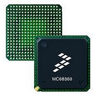
MC68EN360CAI25L Freescale Semiconductor, MC68EN360CAI25L Datasheet - Page 369

MC68EN360CAI25L
Manufacturer Part Number
MC68EN360CAI25L
Description
IC MPU QUICC 25MHZ 240-FQFP
Manufacturer
Freescale Semiconductor
Series
MC68000r
Datasheets
1.MC68EN302AG20BT.pdf
(8 pages)
2.MC68EN360VR25L.pdf
(14 pages)
3.MC68EN360VR25L.pdf
(2 pages)
4.MC68EN360CAI25L.pdf
(962 pages)
Specifications of MC68EN360CAI25L
Processor Type
M683xx 32-Bit
Speed
25MHz
Voltage
5V
Mounting Type
Surface Mount
Package / Case
240-FQFP
Core Size
32 Bit
Cpu Speed
25MHz
Embedded Interface Type
SCP, TDM
Digital Ic Case Style
FQFP
No. Of Pins
240
Supply Voltage Range
4.75V To 5.25V
Rohs Compliant
Yes
Family Name
M68xxx
Device Core
ColdFire
Device Core Size
32b
Frequency (max)
25MHz
Instruction Set Architecture
RISC
Supply Voltage 1 (typ)
5V
Operating Supply Voltage (max)
5.25V
Operating Supply Voltage (min)
4.75V
Operating Temp Range
-40C to 85C
Operating Temperature Classification
Industrial
Mounting
Surface Mount
Pin Count
240
Package Type
FQFP
Lead Free Status / RoHS Status
Lead free / RoHS Compliant
Features
-
Lead Free Status / Rohs Status
Compliant
Available stocks
Company
Part Number
Manufacturer
Quantity
Price
Company:
Part Number:
MC68EN360CAI25L
Manufacturer:
APLHA
Quantity:
12 000
Company:
Part Number:
MC68EN360CAI25L
Manufacturer:
Freescale Semiconductor
Quantity:
10 000
Part Number:
MC68EN360CAI25L
Manufacturer:
FREESCALE
Quantity:
20 000
- MC68EN302AG20BT PDF datasheet
- MC68EN360VR25L PDF datasheet #2
- MC68EN360VR25L PDF datasheet #3
- MC68EN360CAI25L PDF datasheet #4
- Current page: 369 of 962
- Download datasheet (4Mb)
Freescale Semiconductor, Inc.
IDMA Channels
The relative priority between the two IDMAs and SDMA channels is user programmable.
Regardless of the system configuration, if the SDMA is a bus master when a higher priority
IDMA channel needs to transfer over the bus, the IDMA will steal cycles from the SDMA with
no arbitration overhead.
When the QUICC is in slave mode (CPU32+ disabled), the IDMA can steal cycles from the
SDMA with no arbitration overhead. See Section 4 Bus Operation for diagrams of bus arbi-
tration by an internal master in slave mode.
Additionally, when the QUICC is in slave mode, the BCLRI pin can be used to force the
IDMA and other internal bus masters off the bus. The BCLRI pin is assigned an arbitration
ID in slave mode to allow a selection of which internal bus masters are allowed to be forced
off the bus. An application of this capability is to connect the BCLRO pin of a QUICC in nor-
mal operation to the BCLRI pin of a QUICC in slave mode. This configuration allows the user
to implement capabilities such as giving all SDMA channels priority over all IDMA channels
in the system.
7.6.4.6 IDMA OPERAND TRANSFERS. Once the IDMA successfully arbitrates for the bus,
it can begin making operand transfers. The source IDMA bus cycle has timing identical to
an internal master read bus cycle. The destination IDMA bus cycle has timing identical to an
internal master write bus cycle.
The two-channel IDMA module supports dual and single address transfers. The dual
address operand transfer consists of a source operand read and a destination operand
write. Each single address operand transfer consists of one external bus cycle, which allows
either a read or a write cycle to occur.
7.6.4.6.1 Dual Address Mode. The two IDMA channels can each be programmed to oper-
ate in a dual address transfer mode (see Figure 7-13). In this mode, the operand is read from
the source address specified in the SAPR and placed in the DHR. The operand read may
take up to four bus cycles to complete because of differences in operand sizes of the source
and destination. The operand is then written to the address specified in the DAPR. This
transfer may also be up to four bus cycles long. In this manner, various combinations of
peripheral, memory, and operand sizes may be used.
The dual address transfers can be started either by the internal request mode or by an exter-
nal device using DREQx. When the external device uses DREQx, the channel can be pro-
grammed to operate in either the cycle steal or burst transfer modes. See 7.6.4.4.3 External
Burst Mode and 7.6.4.4.4 External Cycle Steal for information about these modes.
Dual Address Source Read . During this type of IDMA cycle, the SAPR drives the address
bus, the FCR drives the source function codes, and the CMR drives the size control. Data
is read from the memory or peripheral and placed in the DHR when the bus cycle is termi-
nated. When the complete operand has been read, the SAPR is incremented by 1, 2, or 4,
depending on the address and size information specified by the SAPI and SSIZE bits of the
CMR. See 7.6.2.3 Source Address Pointer Register (SAPR) for more information.
MC68360 USER’S MANUAL
For More Information On This Product,
Go to: www.freescale.com
Related parts for MC68EN360CAI25L
Image
Part Number
Description
Manufacturer
Datasheet
Request
R
Part Number:
Description:
Manufacturer:
Freescale Semiconductor, Inc
Datasheet:
Part Number:
Description:
Manufacturer:
Freescale Semiconductor, Inc
Datasheet:
Part Number:
Description:
Manufacturer:
Freescale Semiconductor, Inc
Datasheet:
Part Number:
Description:
Manufacturer:
Freescale Semiconductor, Inc
Datasheet:
Part Number:
Description:
Manufacturer:
Freescale Semiconductor, Inc
Datasheet:
Part Number:
Description:
Manufacturer:
Freescale Semiconductor, Inc
Datasheet:
Part Number:
Description:
Manufacturer:
Freescale Semiconductor, Inc
Datasheet:
Part Number:
Description:
Manufacturer:
Freescale Semiconductor, Inc
Datasheet:
Part Number:
Description:
Manufacturer:
Freescale Semiconductor, Inc
Datasheet:
Part Number:
Description:
Manufacturer:
Freescale Semiconductor, Inc
Datasheet:
Part Number:
Description:
Manufacturer:
Freescale Semiconductor, Inc
Datasheet:
Part Number:
Description:
Manufacturer:
Freescale Semiconductor, Inc
Datasheet:
Part Number:
Description:
Manufacturer:
Freescale Semiconductor, Inc
Datasheet:
Part Number:
Description:
Manufacturer:
Freescale Semiconductor, Inc
Datasheet:
Part Number:
Description:
Manufacturer:
Freescale Semiconductor, Inc
Datasheet:


