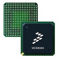
MC68EN360CAI25L Freescale Semiconductor, MC68EN360CAI25L Datasheet - Page 113

MC68EN360CAI25L
Manufacturer Part Number
MC68EN360CAI25L
Description
IC MPU QUICC 25MHZ 240-FQFP
Manufacturer
Freescale Semiconductor
Series
MC68000r
Datasheets
1.MC68EN302AG20BT.pdf
(8 pages)
2.MC68EN360VR25L.pdf
(14 pages)
3.MC68EN360VR25L.pdf
(2 pages)
4.MC68EN360CAI25L.pdf
(962 pages)
Specifications of MC68EN360CAI25L
Processor Type
M683xx 32-Bit
Speed
25MHz
Voltage
5V
Mounting Type
Surface Mount
Package / Case
240-FQFP
Core Size
32 Bit
Cpu Speed
25MHz
Embedded Interface Type
SCP, TDM
Digital Ic Case Style
FQFP
No. Of Pins
240
Supply Voltage Range
4.75V To 5.25V
Rohs Compliant
Yes
Family Name
M68xxx
Device Core
ColdFire
Device Core Size
32b
Frequency (max)
25MHz
Instruction Set Architecture
RISC
Supply Voltage 1 (typ)
5V
Operating Supply Voltage (max)
5.25V
Operating Supply Voltage (min)
4.75V
Operating Temp Range
-40C to 85C
Operating Temperature Classification
Industrial
Mounting
Surface Mount
Pin Count
240
Package Type
FQFP
Lead Free Status / RoHS Status
Lead free / RoHS Compliant
Features
-
Lead Free Status / Rohs Status
Compliant
Available stocks
Company
Part Number
Manufacturer
Quantity
Price
Company:
Part Number:
MC68EN360CAI25L
Manufacturer:
APLHA
Quantity:
12 000
Company:
Part Number:
MC68EN360CAI25L
Manufacturer:
Freescale Semiconductor
Quantity:
10 000
Part Number:
MC68EN360CAI25L
Manufacturer:
FREESCALE
Quantity:
20 000
- MC68EN302AG20BT PDF datasheet
- MC68EN360VR25L PDF datasheet #2
- MC68EN360VR25L PDF datasheet #3
- MC68EN360CAI25L PDF datasheet #4
- Current page: 113 of 962
- Download datasheet (4Mb)
The interrupt acknowledge cycle is a read cycle. It differs from the read cycle described in
4.3.1 Read Cycle in that it accesses the CPU address space. Specifically, the differences
are as follows:
The responding device places the vector number on the data bus during the interrupt
acknowledge cycle. Beyond this, the cycle is terminated normally with DSACKx.
Figure 4-26 is a flowchart of the interrupt acknowledge cycle; Figure 4-27 shows the timing
for an interrupt acknowledge cycle terminated with DSACKx.
1. FC3–FC0 are set to $7 (FC3/FC2/FC1/FC0 = 0111) for CPU address space.
2. A3, A2, and A1 are set to the interrupt request level, and the IACKx strobe correspond-
3. The CPU32+ space type field (A19–A16) is set to $F (interrupt acknowledge).
4. Other address signals (A31–A20, A15–A4, and A0) are set to one.
ing to the current interrupt level is asserted. (Either the function codes and address sig-
nals or the IACKx strobes can be monitored to determine that an interrupt
acknowledge cycle is in progress and the current interrupt level.)
1) PLACE VECTOR NUMBER ON LEAST SIGNIFICANT
2) ASSERT DSACKx (OR AVEC IF NO VECTOR
1) NEGATE DSACKx
BYTE OF DATA PORT (DEPENDS ON
PORT SIZE)
NUMBER)
PROVIDE VECTOR NUMBER
INTERRUPTING DEVICE
REQUEST INTERRUPT
Figure 4-26. Interrupt Acknowledge Cycle Flowchart
RELEASE
Freescale Semiconductor, Inc.
For More Information On This Product,
MC68360 USER’S MANUAL
Go to: www.freescale.com
1) SYNCHRONIZE IRQ7–IRQ1
2) COMPARE IRQ7–IRQ1 TO MASK LEVEL AND
3) ASSERT BCLRO
4) PLACE INTERRUPT LEVEL ON A1–A3;
5) SET R/W TO READ
6) SET FC3–FC0 TO 0111
7) DRIVE SIZx PINS TO INDICATE A ONE-BYTE
8) NEGATE BCLRO.
9) ASSERT AS, DS, AND OE
1) LATCH VECTOR NUMBER
2) NEGATE AS, DS, AND OE
WAIT FOR INSTRUCTION TO COMPLETE
TYPE FIELD (A19–A16) = $F
TRANSFER
ACQUIRE VECTOR NUMBER
START NEXT CYCLE
GRANT INTERRUPT
QUICC
Bus Operation
Related parts for MC68EN360CAI25L
Image
Part Number
Description
Manufacturer
Datasheet
Request
R
Part Number:
Description:
Manufacturer:
Freescale Semiconductor, Inc
Datasheet:
Part Number:
Description:
Manufacturer:
Freescale Semiconductor, Inc
Datasheet:
Part Number:
Description:
Manufacturer:
Freescale Semiconductor, Inc
Datasheet:
Part Number:
Description:
Manufacturer:
Freescale Semiconductor, Inc
Datasheet:
Part Number:
Description:
Manufacturer:
Freescale Semiconductor, Inc
Datasheet:
Part Number:
Description:
Manufacturer:
Freescale Semiconductor, Inc
Datasheet:
Part Number:
Description:
Manufacturer:
Freescale Semiconductor, Inc
Datasheet:
Part Number:
Description:
Manufacturer:
Freescale Semiconductor, Inc
Datasheet:
Part Number:
Description:
Manufacturer:
Freescale Semiconductor, Inc
Datasheet:
Part Number:
Description:
Manufacturer:
Freescale Semiconductor, Inc
Datasheet:
Part Number:
Description:
Manufacturer:
Freescale Semiconductor, Inc
Datasheet:
Part Number:
Description:
Manufacturer:
Freescale Semiconductor, Inc
Datasheet:
Part Number:
Description:
Manufacturer:
Freescale Semiconductor, Inc
Datasheet:
Part Number:
Description:
Manufacturer:
Freescale Semiconductor, Inc
Datasheet:
Part Number:
Description:
Manufacturer:
Freescale Semiconductor, Inc
Datasheet:


