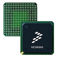
MC68EN360CAI25L Freescale Semiconductor, MC68EN360CAI25L Datasheet - Page 60

MC68EN360CAI25L
Manufacturer Part Number
MC68EN360CAI25L
Description
IC MPU QUICC 25MHZ 240-FQFP
Manufacturer
Freescale Semiconductor
Series
MC68000r
Datasheets
1.MC68EN302AG20BT.pdf
(8 pages)
2.MC68EN360VR25L.pdf
(14 pages)
3.MC68EN360VR25L.pdf
(2 pages)
4.MC68EN360CAI25L.pdf
(962 pages)
Specifications of MC68EN360CAI25L
Processor Type
M683xx 32-Bit
Speed
25MHz
Voltage
5V
Mounting Type
Surface Mount
Package / Case
240-FQFP
Core Size
32 Bit
Cpu Speed
25MHz
Embedded Interface Type
SCP, TDM
Digital Ic Case Style
FQFP
No. Of Pins
240
Supply Voltage Range
4.75V To 5.25V
Rohs Compliant
Yes
Family Name
M68xxx
Device Core
ColdFire
Device Core Size
32b
Frequency (max)
25MHz
Instruction Set Architecture
RISC
Supply Voltage 1 (typ)
5V
Operating Supply Voltage (max)
5.25V
Operating Supply Voltage (min)
4.75V
Operating Temp Range
-40C to 85C
Operating Temperature Classification
Industrial
Mounting
Surface Mount
Pin Count
240
Package Type
FQFP
Lead Free Status / RoHS Status
Lead free / RoHS Compliant
Features
-
Lead Free Status / Rohs Status
Compliant
Available stocks
Company
Part Number
Manufacturer
Quantity
Price
Company:
Part Number:
MC68EN360CAI25L
Manufacturer:
APLHA
Quantity:
12 000
Company:
Part Number:
MC68EN360CAI25L
Manufacturer:
Freescale Semiconductor
Quantity:
10 000
Part Number:
MC68EN360CAI25L
Manufacturer:
FREESCALE
Quantity:
20 000
- MC68EN302AG20BT PDF datasheet
- MC68EN360VR25L PDF datasheet #2
- MC68EN360VR25L PDF datasheet #3
- MC68EN360CAI25L PDF datasheet #4
- Current page: 60 of 962
- Download datasheet (4Mb)
Freescale Semiconductor, Inc.
Signal Descriptions
signal is the serial clock used to transfer commands/status to and from the CPU32+ during
background debug mode.
2.1.11.5 FREEZE/INITIAL CONFIGURATION (FREEZE/CONFIG2). This pin can be pro-
grammed as the freeze output or as the initial configuration pin 2 input signal during system
reset.
FREEZE—Assertion of this active-high output signal indicates that the CPU32+ has
acknowledged a breakpoint and has initiated background mode operation.
CONFIG2—See 2.1.13 Initial Configuration Pins (CONFIG) for the description.
2.1.12 Test Signals
The following signals are used with the on-board test logic . See Section 8 Scan Chain Test
Access Port for more information on the use of these signals.
2.1.12.1 TRI-STATE SIGNAL (TRIS). TThe TRIS pin is enabled as a tristate control pin
only when the CPU32+ is enabled, and it is not sampled during reset. When asserted, TRIS
immediately tristates the pins.
2.1.12.2 TEST RESET (TRST). This input provides asynchronous reset to the test logic.
2.1.12.3 TEST CLOCK (TCK). This input provides a clock for on-board test logic.
2.1.12.4 TEST MODE SELECT (TMS). This input controls test mode operations for on-
board test logic.
2.1.12.5 TEST DATA IN (TDI). This input is used for serial test instructions and test data
for on-board test logic.
2.1.12.6 TEST DATA OUT (TDO). This output is used for serial test instructions and test
data for on-board test logic.
2.1.13 Initial Configuration Pins (CONFIG)
The CONFIG2–CONFIG0 pins select the QUICC initial configuration during reset (see Table
2-6). They decide whether the CPU32+ core will be enabled or disabled, the global chip
select port will be 8-, 16-, or 32-bits, and the MBAR address will be $003FF00 or
$0033FF04. After reset, these pins may be programmed to their other function. The
CONFIG2–CONFIG0 lines have internal pullup resistors so that if they are left floating, the
default selection will be 111. See Section 6 System Integration Module (SIM60) for more
information.
2-12
MC68360 USER’S MANUAL
For More Information On This Product,
Go to: www.freescale.com
Related parts for MC68EN360CAI25L
Image
Part Number
Description
Manufacturer
Datasheet
Request
R
Part Number:
Description:
Manufacturer:
Freescale Semiconductor, Inc
Datasheet:
Part Number:
Description:
Manufacturer:
Freescale Semiconductor, Inc
Datasheet:
Part Number:
Description:
Manufacturer:
Freescale Semiconductor, Inc
Datasheet:
Part Number:
Description:
Manufacturer:
Freescale Semiconductor, Inc
Datasheet:
Part Number:
Description:
Manufacturer:
Freescale Semiconductor, Inc
Datasheet:
Part Number:
Description:
Manufacturer:
Freescale Semiconductor, Inc
Datasheet:
Part Number:
Description:
Manufacturer:
Freescale Semiconductor, Inc
Datasheet:
Part Number:
Description:
Manufacturer:
Freescale Semiconductor, Inc
Datasheet:
Part Number:
Description:
Manufacturer:
Freescale Semiconductor, Inc
Datasheet:
Part Number:
Description:
Manufacturer:
Freescale Semiconductor, Inc
Datasheet:
Part Number:
Description:
Manufacturer:
Freescale Semiconductor, Inc
Datasheet:
Part Number:
Description:
Manufacturer:
Freescale Semiconductor, Inc
Datasheet:
Part Number:
Description:
Manufacturer:
Freescale Semiconductor, Inc
Datasheet:
Part Number:
Description:
Manufacturer:
Freescale Semiconductor, Inc
Datasheet:
Part Number:
Description:
Manufacturer:
Freescale Semiconductor, Inc
Datasheet:


