AT91SAM9G45-EKES Atmel, AT91SAM9G45-EKES Datasheet - Page 1035
AT91SAM9G45-EKES
Manufacturer Part Number
AT91SAM9G45-EKES
Description
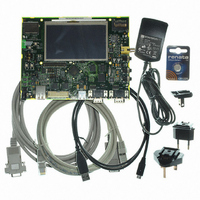
KIT EVAL FOR AT91SAM9G45
Manufacturer
Atmel
Series
AT91SAM Smart ARMr
Type
MCUr
Datasheets
1.AT91SAM9G45-EKES.pdf
(56 pages)
2.AT91SAM9G45-EKES.pdf
(1218 pages)
3.AT91SAM9G45-EKES.pdf
(66 pages)
Specifications of AT91SAM9G45-EKES
Contents
Board
Processor To Be Evaluated
SAM9G45
Data Bus Width
32 bit
Interface Type
I2C, SPI, UART
Maximum Operating Temperature
+ 50 C
Minimum Operating Temperature
- 10 C
Operating Supply Voltage
1.8 V to 3.3 V
For Use With/related Products
AT91SAM9G45
Lead Free Status / RoHS Status
Lead free / RoHS Compliant
Other names
Q4626953


42.6.3
42.6.3.1
42.6.3.2
42.6.3.3
6438F–ATARM–21-Jun-10
PWM Controller Operations
Initialization
Changing the Duty Cycle or the Period
Source Clock Selection Criteria
Before enabling the output channel, this channel must have been configured by the software
application:
It is possible to synchronize different channels by enabling them at the same time by means of
writing simultaneously several CHIDx bits in the PWM_ENA register.
The large number of source clocks can make selection difficult. The relationship between the
value in the Period Register (PWM_CPRDx) and the Duty Cycle Register (PWM_CDTYx) can
help the user in choosing. The event number written in the Period Register gives the PWM accu-
racy. The Duty Cycle quantum cannot be lower than 1/PWM_CPRDx value. The higher the value
of PWM_CPRDx, the greater the PWM accuracy.
For example, if the user sets 15 (in decimal) in PWM_CPRDx, the user is able to set a value
between 1 up to 14 in PWM_CDTYx Register. The resulting duty cycle quantum cannot be lower
than 1/15 of the PWM period.
It is possible to modulate the output waveform duty cycle or period.
To prevent unexpected output waveform, the user must use the update register (PWM_CUPDx)
to change waveform parameters while the channel is still enabled. The user can write a new
period value or duty cycle value in the update register (PWM_CUPDx). This register holds the
new value until the end of the current cycle and updates the value for the next cycle. Depending
on the CPD field in the PWM_CMRx register, PWM_CUPDx either updates PWM_CPRDx or
PWM_CDTYx. Note that even if the update register is used, the period must not be smaller than
the duty cycle.
• Configuration of the clock generator if DIVA and DIVB are required
• Selection of the clock for each channel (CPRE field in the PWM_CMRx register)
• Configuration of the waveform alignment for each channel (CALG field in the PWM_CMRx
• Configuration of the period for each channel (CPRD in the PWM_CPRDx register). Writing in
• Configuration of the duty cycle for each channel (CDTY in the PWM_CDTYx register).
• Configuration of the output waveform polarity for each channel (CPOL in the PWM_CMRx
• Enable Interrupts (Writing CHIDx in the PWM_IER register)
• Enable the PWM channel (Writing CHIDx in the PWM_ENA register)
• In such a situation, all channels may have the same clock selector configuration and the
register)
PWM_CPRDx Register is possible while the channel is disabled. After validation of the
channel, the user must use PWM_CUPDx Register to update PWM_CPRDx as explained
below.
Writing in PWM_CDTYx Register is possible while the channel is disabled. After validation of
the channel, the user must use PWM_CUPDx Register to update PWM_CDTYx as explained
below.
register)
same period specified.
AT91SAM9G45
1035
Related parts for AT91SAM9G45-EKES
Image
Part Number
Description
Manufacturer
Datasheet
Request
R

Part Number:
Description:
MCU ARM9 64K SRAM 144-LFBGA
Manufacturer:
Atmel
Datasheet:

Part Number:
Description:
IC ARM7 MCU FLASH 256K 100LQFP
Manufacturer:
Atmel
Datasheet:

Part Number:
Description:
IC ARM9 MPU 217-LFBGA
Manufacturer:
Atmel
Datasheet:
Part Number:
Description:
MCU ARM9 ULTRA LOW PWR 217-LFBGA
Manufacturer:
Atmel
Datasheet:

Part Number:
Description:
MCU ARM9 324-TFBGA
Manufacturer:
Atmel
Datasheet:
Part Number:
Description:
IC MCU ARM9 SAMPLING 217CBGA
Manufacturer:
Atmel
Datasheet:
Part Number:
Description:
IC ARM9 MCU 217-LFBGA
Manufacturer:
Atmel
Datasheet:

Part Number:
Description:
IC ARM9 MCU 208-PQFP
Manufacturer:
Atmel
Datasheet:
Part Number:
Description:
MCU ARM 512K HS FLASH 100-LQFP
Manufacturer:
Atmel
Datasheet:

Part Number:
Description:
MCU ARM 512K HS FLASH 100-TFBGA
Manufacturer:
Atmel
Datasheet:
Part Number:
Description:
IC ARM9 MCU 200 MHZ 324-TFBGA
Manufacturer:
Atmel
Datasheet:

Part Number:
Description:
IC ARM MCU 16BIT 128K 256BGA
Manufacturer:
Atmel
Datasheet:

Part Number:
Description:
IC ARM7 MCU 32BIT 128K 64LQFP
Manufacturer:
Atmel
Datasheet:

Part Number:
Description:
IC ARM7 MCU FLASH 256K 128-LQFP
Manufacturer:
Atmel
Datasheet:
Part Number:
Description:
IC ARM7 MCU FLASH 512K 128-LQFP
Manufacturer:
Atmel
Datasheet: