AT91SAM9G45-EKES Atmel, AT91SAM9G45-EKES Datasheet - Page 425
AT91SAM9G45-EKES
Manufacturer Part Number
AT91SAM9G45-EKES
Description
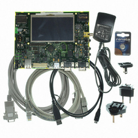
KIT EVAL FOR AT91SAM9G45
Manufacturer
Atmel
Series
AT91SAM Smart ARMr
Type
MCUr
Datasheets
1.AT91SAM9G45-EKES.pdf
(56 pages)
2.AT91SAM9G45-EKES.pdf
(1218 pages)
3.AT91SAM9G45-EKES.pdf
(66 pages)
Specifications of AT91SAM9G45-EKES
Contents
Board
Processor To Be Evaluated
SAM9G45
Data Bus Width
32 bit
Interface Type
I2C, SPI, UART
Maximum Operating Temperature
+ 50 C
Minimum Operating Temperature
- 10 C
Operating Supply Voltage
1.8 V to 3.3 V
For Use With/related Products
AT91SAM9G45
Lead Free Status / RoHS Status
Lead free / RoHS Compliant
Other names
Q4626953


29.6.3
29.6.4
29.7
29.7.1
29.7.2
6438F–ATARM–21-Jun-10
Functional Description
Interrupt
Peripheral DMA Controller (PDMA) Direct Memory Access Controller (DMAC)
Modes of Operation
Data Transfer
The SPI interface has an interrupt line connected to the Advanced Interrupt Controller
(AIC).Handling the SPI interrupt requires programming the AIC before configuring the SPI.
Table 29-3.
The SPI interface can be used in conjunction with the PDMA DMAC in order to reduce processor
overhead. For a full description of the PDMA DMAC, refer to the corresponding section in the full
datasheet.
The SPI operates in Master Mode or in Slave Mode.
Operation in Master Mode is programmed by writing at 1 the MSTR bit in the Mode Register.
The pins NPCS0 to NPCS3 are all configured as outputs, the SPCK pin is driven, the MISO line
is wired on the receiver input and the MOSI line driven as an output by the transmitter.
If the MSTR bit is written at 0, the SPI operates in Slave Mode. The MISO line is driven by the
transmitter output, the MOSI line is wired on the receiver input, the SPCK pin is driven by the
transmitter to synchronize the receiver. The NPCS0 pin becomes an input, and is used as a
Slave Select signal (NSS). The pins NPCS1 to NPCS3 are not driven and can be used for other
purposes.
The data transfers are identically programmable for both modes of operations. The baud rate
generator is activated only in Master Mode.
Four combinations of polarity and phase are available for data transfers. The clock polarity is
programmed with the CPOL bit in the Chip Select Register. The clock phase is programmed with
the NCPHA bit. These two parameters determine the edges of the clock signal on which data is
driven and sampled. Each of the two parameters has two possible states, resulting in four possi-
ble combinations that are incompatible with one another. Thus, a master/slave pair must use the
same parameter pair values to communicate. If multiple slaves are used and fixed in different
configurations, the master must reconfigure itself each time it needs to communicate with a dif-
ferent slave.
Instance
SPI0
SPI1
Peripheral IDs
14
15
ID
AT91SAM9G45
425
Related parts for AT91SAM9G45-EKES
Image
Part Number
Description
Manufacturer
Datasheet
Request
R

Part Number:
Description:
MCU ARM9 64K SRAM 144-LFBGA
Manufacturer:
Atmel
Datasheet:

Part Number:
Description:
IC ARM7 MCU FLASH 256K 100LQFP
Manufacturer:
Atmel
Datasheet:

Part Number:
Description:
IC ARM9 MPU 217-LFBGA
Manufacturer:
Atmel
Datasheet:
Part Number:
Description:
MCU ARM9 ULTRA LOW PWR 217-LFBGA
Manufacturer:
Atmel
Datasheet:

Part Number:
Description:
MCU ARM9 324-TFBGA
Manufacturer:
Atmel
Datasheet:
Part Number:
Description:
IC MCU ARM9 SAMPLING 217CBGA
Manufacturer:
Atmel
Datasheet:
Part Number:
Description:
IC ARM9 MCU 217-LFBGA
Manufacturer:
Atmel
Datasheet:

Part Number:
Description:
IC ARM9 MCU 208-PQFP
Manufacturer:
Atmel
Datasheet:
Part Number:
Description:
MCU ARM 512K HS FLASH 100-LQFP
Manufacturer:
Atmel
Datasheet:

Part Number:
Description:
MCU ARM 512K HS FLASH 100-TFBGA
Manufacturer:
Atmel
Datasheet:
Part Number:
Description:
IC ARM9 MCU 200 MHZ 324-TFBGA
Manufacturer:
Atmel
Datasheet:

Part Number:
Description:
IC ARM MCU 16BIT 128K 256BGA
Manufacturer:
Atmel
Datasheet:

Part Number:
Description:
IC ARM7 MCU 32BIT 128K 64LQFP
Manufacturer:
Atmel
Datasheet:

Part Number:
Description:
IC ARM7 MCU FLASH 256K 128-LQFP
Manufacturer:
Atmel
Datasheet:
Part Number:
Description:
IC ARM7 MCU FLASH 512K 128-LQFP
Manufacturer:
Atmel
Datasheet: