AT91SAM9G45-EKES Atmel, AT91SAM9G45-EKES Datasheet - Page 258
AT91SAM9G45-EKES
Manufacturer Part Number
AT91SAM9G45-EKES
Description
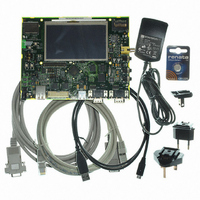
KIT EVAL FOR AT91SAM9G45
Manufacturer
Atmel
Series
AT91SAM Smart ARMr
Type
MCUr
Datasheets
1.AT91SAM9G45-EKES.pdf
(56 pages)
2.AT91SAM9G45-EKES.pdf
(1218 pages)
3.AT91SAM9G45-EKES.pdf
(66 pages)
Specifications of AT91SAM9G45-EKES
Contents
Board
Processor To Be Evaluated
SAM9G45
Data Bus Width
32 bit
Interface Type
I2C, SPI, UART
Maximum Operating Temperature
+ 50 C
Minimum Operating Temperature
- 10 C
Operating Supply Voltage
1.8 V to 3.3 V
For Use With/related Products
AT91SAM9G45
Lead Free Status / RoHS Status
Lead free / RoHS Compliant
Other names
Q4626953


22.6
Figure 22-26. Programmable IO Delays
22.7
The User Interface is connected to the APB bus.
258
Programmable IO Delays
DDR-SDRAM Controller (DDRSDRC) User Interface
AT91SAM9G45
SMC
The external bus interface consists of a data bus, an address bus and control signals. The simul-
taneous switching outputs on these busses may lead to a peak of current in the internal and
external power supply lines.
In order to reduce the peak of current in such cases, additional propagation delays can be
a d j u s t e d i n d e p e n d e n t l y f o r p a d b u f f e r s b y m e a n s o f c o n f i g u r a t i o n r e g i s t e r s ,
DDRSDRC_DELAY1-8.
The additional programmable delays for each IO range from 0 to
delay can differ between IOs supporting this feature. Delay can be modified per programming for
each IO. The minimal additional delay that can be programmed on a PAD supporting this feature
is 1/16 of the maximum programmable delay.
When programming 0x0 in fields “Delay1 to Delay8”, no delay is added (reset value) and the
propagation delay of the pad buffers is the inherent delay of the pad buffer. When programming
0xF in field “Delay1” the propagation delay of the corresponding pad is maximal.
D D R S D R C _ D E L A Y 1 , D D R S D R C _ D E L A Y 2 a l l o w t o c o n f i g u r e d e l a y o n D [ 1 5 : 0 ] ,
DDRSDRC_DELAY1[3:0] corresponds to D[0] and DDRSDRC_DELAY2[3:0] corresponds to
D[8].
D D R S D R C _ D E L A Y 3 , D D R S D R C _ D E L A Y 4 a l l o w t o c o n f i g u r e d e l a y o n A 1 3 : 0 ] ,
DDRSDRC_DELAY3[3:0] corresponds to A[0] and DDRSDRC_DELAY4[3:0] corresponds to
A[8].
DELAY1
DELAYx
DELAYy
DELAY2
D_out[0]
D_out[1]
D_out[n]
D_in[0]
D_in[1]
D_in[n]
A[m]
Programmable Delay Line
Programmable Delay Line
Programmable Delay Line
Programmable Delay Line
4
ns (Worst Case PVT). The
D[0]
D[1]
D[n]
A[m]
6438F–ATARM–21-Jun-10
Related parts for AT91SAM9G45-EKES
Image
Part Number
Description
Manufacturer
Datasheet
Request
R

Part Number:
Description:
MCU ARM9 64K SRAM 144-LFBGA
Manufacturer:
Atmel
Datasheet:

Part Number:
Description:
IC ARM7 MCU FLASH 256K 100LQFP
Manufacturer:
Atmel
Datasheet:

Part Number:
Description:
IC ARM9 MPU 217-LFBGA
Manufacturer:
Atmel
Datasheet:
Part Number:
Description:
MCU ARM9 ULTRA LOW PWR 217-LFBGA
Manufacturer:
Atmel
Datasheet:

Part Number:
Description:
MCU ARM9 324-TFBGA
Manufacturer:
Atmel
Datasheet:
Part Number:
Description:
IC MCU ARM9 SAMPLING 217CBGA
Manufacturer:
Atmel
Datasheet:
Part Number:
Description:
IC ARM9 MCU 217-LFBGA
Manufacturer:
Atmel
Datasheet:

Part Number:
Description:
IC ARM9 MCU 208-PQFP
Manufacturer:
Atmel
Datasheet:
Part Number:
Description:
MCU ARM 512K HS FLASH 100-LQFP
Manufacturer:
Atmel
Datasheet:

Part Number:
Description:
MCU ARM 512K HS FLASH 100-TFBGA
Manufacturer:
Atmel
Datasheet:
Part Number:
Description:
IC ARM9 MCU 200 MHZ 324-TFBGA
Manufacturer:
Atmel
Datasheet:

Part Number:
Description:
IC ARM MCU 16BIT 128K 256BGA
Manufacturer:
Atmel
Datasheet:

Part Number:
Description:
IC ARM7 MCU 32BIT 128K 64LQFP
Manufacturer:
Atmel
Datasheet:

Part Number:
Description:
IC ARM7 MCU FLASH 256K 128-LQFP
Manufacturer:
Atmel
Datasheet:
Part Number:
Description:
IC ARM7 MCU FLASH 512K 128-LQFP
Manufacturer:
Atmel
Datasheet: