AT91SAM9G45-EKES Atmel, AT91SAM9G45-EKES Datasheet - Page 201
AT91SAM9G45-EKES
Manufacturer Part Number
AT91SAM9G45-EKES
Description
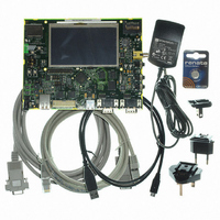
KIT EVAL FOR AT91SAM9G45
Manufacturer
Atmel
Series
AT91SAM Smart ARMr
Type
MCUr
Datasheets
1.AT91SAM9G45-EKES.pdf
(56 pages)
2.AT91SAM9G45-EKES.pdf
(1218 pages)
3.AT91SAM9G45-EKES.pdf
(66 pages)
Specifications of AT91SAM9G45-EKES
Contents
Board
Processor To Be Evaluated
SAM9G45
Data Bus Width
32 bit
Interface Type
I2C, SPI, UART
Maximum Operating Temperature
+ 50 C
Minimum Operating Temperature
- 10 C
Operating Supply Voltage
1.8 V to 3.3 V
For Use With/related Products
AT91SAM9G45
Lead Free Status / RoHS Status
Lead free / RoHS Compliant
Other names
Q4626953


Figure 21-16. Chip Select Wait State between a Read Access on NCS0 and a Write Access on NCS2
21.9.2
6438F–ATARM–21-Jun-10
Early Read Wait State
NBS0, NBS1,
NBS2, NBS3,
A0,A1
A[25:2]
D[31:0]
NCS0
NCS2
NWE
MCK
NRD
In some cases, the SMC inserts a wait state cycle between a write access and a read access to
allow time for the write cycle to end before the subsequent read cycle begins. This wait state is
not generated in addition to a chip select wait state. The early read cycle thus only occurs
between a write and read access to the same memory device (same chip select).
An early read wait state is automatically inserted if at least one of the following conditions is
valid:
• if the write controlling signal has no hold time and the read controlling signal has no setup
• in NCS write controlled mode (WRITE_MODE = 0), if there is no hold timing on the NCS
• in NWE controlled mode (WRITE_MODE = 1) and if there is no hold timing (NWE_HOLD =
time
signal and the NCS_RD_SETUP parameter is set to 0, regardless of the read mode
21-18). The write operation must end with a NCS rising edge. Without an Early Read Wait
State, the write operation could not complete properly.
0), the feedback of the write control signal is used to control address, data, chip select and
byte select lines. If the external write control signal is not inactivated as expected due to load
capacitances, an Early Read Wait State is inserted and address, data and control signals are
maintained one more cycle. See
(Figure
NRD_CYCLE
21-17).
Read to Write
Wait State
Figure
21-19.
Chip Select
Wait State
NWE_CYCLE
AT91SAM9G45
(Figure
201
Related parts for AT91SAM9G45-EKES
Image
Part Number
Description
Manufacturer
Datasheet
Request
R

Part Number:
Description:
MCU ARM9 64K SRAM 144-LFBGA
Manufacturer:
Atmel
Datasheet:

Part Number:
Description:
IC ARM7 MCU FLASH 256K 100LQFP
Manufacturer:
Atmel
Datasheet:

Part Number:
Description:
IC ARM9 MPU 217-LFBGA
Manufacturer:
Atmel
Datasheet:
Part Number:
Description:
MCU ARM9 ULTRA LOW PWR 217-LFBGA
Manufacturer:
Atmel
Datasheet:

Part Number:
Description:
MCU ARM9 324-TFBGA
Manufacturer:
Atmel
Datasheet:
Part Number:
Description:
IC MCU ARM9 SAMPLING 217CBGA
Manufacturer:
Atmel
Datasheet:
Part Number:
Description:
IC ARM9 MCU 217-LFBGA
Manufacturer:
Atmel
Datasheet:

Part Number:
Description:
IC ARM9 MCU 208-PQFP
Manufacturer:
Atmel
Datasheet:
Part Number:
Description:
MCU ARM 512K HS FLASH 100-LQFP
Manufacturer:
Atmel
Datasheet:

Part Number:
Description:
MCU ARM 512K HS FLASH 100-TFBGA
Manufacturer:
Atmel
Datasheet:
Part Number:
Description:
IC ARM9 MCU 200 MHZ 324-TFBGA
Manufacturer:
Atmel
Datasheet:

Part Number:
Description:
IC ARM MCU 16BIT 128K 256BGA
Manufacturer:
Atmel
Datasheet:

Part Number:
Description:
IC ARM7 MCU 32BIT 128K 64LQFP
Manufacturer:
Atmel
Datasheet:

Part Number:
Description:
IC ARM7 MCU FLASH 256K 128-LQFP
Manufacturer:
Atmel
Datasheet:
Part Number:
Description:
IC ARM7 MCU FLASH 512K 128-LQFP
Manufacturer:
Atmel
Datasheet: