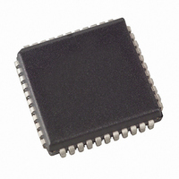
AT89LP6440-20JU Atmel, AT89LP6440-20JU Datasheet - Page 101

AT89LP6440-20JU
Manufacturer Part Number
AT89LP6440-20JU
Description
MCU 8051 64K FLASH ISP 44PLCC
Manufacturer
Atmel
Series
89LPr
Datasheet
1.AT89LP6440-20MU.pdf
(194 pages)
Specifications of AT89LP6440-20JU
Core Processor
8051
Core Size
8-Bit
Speed
20MHz
Connectivity
I²C, SPI, UART/USART
Peripherals
Brown-out Detect/Reset, POR, PWM, WDT
Number Of I /o
38
Program Memory Size
64KB (64K x 8)
Program Memory Type
FLASH
Eeprom Size
8K x 8
Ram Size
4.25K x 8
Voltage - Supply (vcc/vdd)
2.4 V ~ 3.6 V
Data Converters
A/D 8x10b
Oscillator Type
Internal
Operating Temperature
-40°C ~ 85°C
Package / Case
44-PLCC
Processor Series
AT89x
Core
8051
Data Bus Width
8 bit
Data Ram Size
8 KB
Interface Type
2-Wire, SPI
Maximum Clock Frequency
24 MHz
Number Of Programmable I/os
38
Number Of Timers
3
Operating Supply Voltage
2.7 V to 3.6 V
Maximum Operating Temperature
+ 85 C
Mounting Style
SMD/SMT
3rd Party Development Tools
PK51, CA51, A51, ULINK2
Development Tools By Supplier
AT89ISP
Minimum Operating Temperature
- 40 C
On-chip Adc
10 bit, 8 Channel
On-chip Dac
10 bit, 8 Channel
Lead Free Status / RoHS Status
Lead free / RoHS Compliant
Available stocks
Company
Part Number
Manufacturer
Quantity
Price
Company:
Part Number:
AT89LP6440-20JU
Manufacturer:
Atmel
Quantity:
103
Table 17-2.
3706A–MICRO–9/09
SPCR Address = E9H
Not Bit Addressable
Symbol
TSCK
SPE
DORD
MSTR
CPOL
CPHA
Bit
TSCK
SCK Clock Mode. When TSCK = 0, the SCK baud rate is based on the system clock, divided by the SPR
TSCK = 1, the SCK baud rate is based on the Timer 1 overflow rate, divided by the SPR
SPI enable. SPI = 1 enables the SPI channel and connects SS, MOSI, MISO and SCK to pins P1.4, P1.5, P1.6, and P1.7.
SPI = 0 disables the SPI channel.
Data order. DORD = 1 selects LSB first data transmission. DORD = 0 selects MSB first data transmission.
Master/slave select. MSTR = 1 selects Master SPI mode. MSTR = 0 selects slave SPI mode.
Clock polarity. When CPOL = 1, SCK is high when idle. When CPOL = 0, SCK of the master device is low when not
transmitting. Please refer to figure on SPI clock phase and polarity control.
Clock phase. The CPHA bit together with the CPOL bit controls the clock and data relationship between master and
slave. Please refer to figure on SPI clock phase and polarity control.
Function
7
SPCR – SPI Control Register
SPE
.
Table 17-1.
Notes:
6
MOSI
MISO
SCK
Pin
1. In these modes MOSI is active only during transfers. MOSI will be pulled high between trans-
2. In Push-Pull mode MOSI is active only during transfers, otherwise it is tristated to prevent line
fers to allow other masters to control the line.
contention. A weak external pull-up may be required to prevent MOSI from floating.
Mode
Quasi-bidirectional
Push-Pull Output
Input-Only
Open-Drain Output
Quasi-bidirectional
Push-Pull Output
Input-Only
Open-Drain Output
Quasi-bidirectional
Push-Pull Output
Input-Only
Open-Drain Output
DORD
5
SPI Pin Configuration and Behavior when SPE = 1
MSTR
4
Master (MSTR = 1)
No output (Tristated)
No output (Tristated)
Output
Output
Output
Output
Output
Output
Input (Internal Pull-up)
Input (Tristate)
Input (Tristate)
Input (External Pull-up)
(1)
(2)
(1)
CPOL
3
AT89LP6440 - Preliminary
CPHA
2
Slave (MSTR = 0)
Input (Internal Pull-up)
Input (Tristate)
Input (Tristate)
Input (External Pull-up)
Input (Internal Pull-up)
Input (Tristate)
Input (Tristate)
Input (External Pull-up)
Output (SS = 0)
Internal Pull-up (SS = 1 or DISSO = 1)
Output (SS = 0)
Tristated (SS = 1 or DISSO = 1)
No output (Tristated)
Output (SS = 0)
External Pull-up (SS = 1 or DISSO = 1)
Reset Value = 0000 0000B
1-0
SPR1
1
ratio.
SPR0
1-0
0
ratio.When
101


