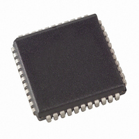
AT89LP6440-20JU Atmel, AT89LP6440-20JU Datasheet - Page 155

AT89LP6440-20JU
Manufacturer Part Number
AT89LP6440-20JU
Description
MCU 8051 64K FLASH ISP 44PLCC
Manufacturer
Atmel
Series
89LPr
Datasheet
1.AT89LP6440-20MU.pdf
(194 pages)
Specifications of AT89LP6440-20JU
Core Processor
8051
Core Size
8-Bit
Speed
20MHz
Connectivity
I²C, SPI, UART/USART
Peripherals
Brown-out Detect/Reset, POR, PWM, WDT
Number Of I /o
38
Program Memory Size
64KB (64K x 8)
Program Memory Type
FLASH
Eeprom Size
8K x 8
Ram Size
4.25K x 8
Voltage - Supply (vcc/vdd)
2.4 V ~ 3.6 V
Data Converters
A/D 8x10b
Oscillator Type
Internal
Operating Temperature
-40°C ~ 85°C
Package / Case
44-PLCC
Processor Series
AT89x
Core
8051
Data Bus Width
8 bit
Data Ram Size
8 KB
Interface Type
2-Wire, SPI
Maximum Clock Frequency
24 MHz
Number Of Programmable I/os
38
Number Of Timers
3
Operating Supply Voltage
2.7 V to 3.6 V
Maximum Operating Temperature
+ 85 C
Mounting Style
SMD/SMT
3rd Party Development Tools
PK51, CA51, A51, ULINK2
Development Tools By Supplier
AT89ISP
Minimum Operating Temperature
- 40 C
On-chip Adc
10 bit, 8 Channel
On-chip Dac
10 bit, 8 Channel
Lead Free Status / RoHS Status
Lead free / RoHS Compliant
Available stocks
Company
Part Number
Manufacturer
Quantity
Price
Company:
Part Number:
AT89LP6440-20JU
Manufacturer:
Atmel
Quantity:
103
24. On-Chip Debug System
24.1
3706A–MICRO–9/09
Physical Interface
Table 23-1.
The AT89LP6440 On-Chip Debug (OCD) System uses a two-wire serial interface to control pro-
gram flow; read, modify, and write the system state; and program the nonvolatile memory. The
OCD System has the following features:
The On-Chip Debug System uses a two-wire synchronous serial interface to establish communi-
cation between the target device and the controlling emulator system. The OCD interface is
enabled by clearing the OCD Enable Fuse. The OCD device connections are shown in
24-1. When OCD is enabled, the RST port pin is configured as an input for the Debug Clock
(DCL). Either the XTAL1, XTAL2 or P4.3 pin is configured as a bi-directional data line for the
Debug Data (DDA) depending on the clock source selected. If the Internal RC Oscillator is
selected, XTAL1 is configured as DDA (A).If the External Clock is selected, XTAL2 is configured
as DDA (B). If the Crystal Oscillator is selected, P4.3 is configured as DDA (C).
When designing a system where On-Chip Debug will be used, the following observations must
be considered for correct operation:
TH0
TH1
TH2
TL0
TL1
TL2
TMOD
TWAR
TWBR
TWCR
TWDR
TWSR
WDTCON
WDTRST
• Complete program flow control
• Read-Modify-Write access to all internal SFRs and data memories
• Four hardware program address breakpoints, plus four program/data address breakpoints
• Unlimited program software breakpoints using BREAK instruction
• Break on change in program memory flow
• Break on stack overflow/underflow
• Break on Watchdog overflow
• Break on reset
• Non-intrusive operation
• Programming of nonvolatile memory
Special Function Register Cross Reference
8CH
8DH
CDH
8AH
8BH
CCH
89H
ACH
AEH
AAH
ADH
ABH
A7H
A6H
Table 11-1 on page 50
Table 11-1 on page 50
Section 12.1 on page 60
Table 11-1 on page 50
Table 11-1 on page 50
Section 12.1 on page 60
Table 11-3 on page 54
Table 18-3 on page 111
Table 18-5 on page 112
Table 18-1 on page 111
Table 18-4 on page 112
Table 18-2 on page 111
Table 21-2 on page 142
Table 21-3 on page 142
AT89LP6440 - Preliminary
Figure
155


