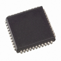
AT89LP6440-20JU Atmel, AT89LP6440-20JU Datasheet - Page 164

AT89LP6440-20JU
Manufacturer Part Number
AT89LP6440-20JU
Description
MCU 8051 64K FLASH ISP 44PLCC
Manufacturer
Atmel
Series
89LPr
Datasheet
1.AT89LP6440-20MU.pdf
(194 pages)
Specifications of AT89LP6440-20JU
Core Processor
8051
Core Size
8-Bit
Speed
20MHz
Connectivity
I²C, SPI, UART/USART
Peripherals
Brown-out Detect/Reset, POR, PWM, WDT
Number Of I /o
38
Program Memory Size
64KB (64K x 8)
Program Memory Type
FLASH
Eeprom Size
8K x 8
Ram Size
4.25K x 8
Voltage - Supply (vcc/vdd)
2.4 V ~ 3.6 V
Data Converters
A/D 8x10b
Oscillator Type
Internal
Operating Temperature
-40°C ~ 85°C
Package / Case
44-PLCC
Processor Series
AT89x
Core
8051
Data Bus Width
8 bit
Data Ram Size
8 KB
Interface Type
2-Wire, SPI
Maximum Clock Frequency
24 MHz
Number Of Programmable I/os
38
Number Of Timers
3
Operating Supply Voltage
2.7 V to 3.6 V
Maximum Operating Temperature
+ 85 C
Mounting Style
SMD/SMT
3rd Party Development Tools
PK51, CA51, A51, ULINK2
Development Tools By Supplier
AT89ISP
Minimum Operating Temperature
- 40 C
On-chip Adc
10 bit, 8 Channel
On-chip Dac
10 bit, 8 Channel
Lead Free Status / RoHS Status
Lead free / RoHS Compliant
Available stocks
Company
Part Number
Manufacturer
Quantity
Price
Company:
Part Number:
AT89LP6440-20JU
Manufacturer:
Atmel
Quantity:
103
25.7
Table 25-5.
Notes:
164
Address
00 – 01h
02 – 03h
04h
05h
06h
07h
08H
09H
0AH
0BH
User Configuration Fuses
1. The default state for all fuses is FFh.
2. Changes to these fuses will only take effect after a device POR.
3. Changes to these fuses will only take effect after the ISP session terminates by bringing RST high.
AT89LP6440 - Preliminary
Fuse Name
Clock Source – CS[0:1]
Start-up Time – SUT[0:1]
Reset Pin Enable
Brown-Out Detector Enable
On-Chip Debug Enable
ISP Enable
User Signature Programming
Tristate Ports
OCD Interface Select
In-Application Programming
User Configuration Fuse Definitions
(3)
The AT89LP6440 includes 11 user fuses for configuration of the device. Each fuse is accessed
at a separate address in the User Fuse Row as listed in
gramming 00h to their locations. Programming FFh to a fuse location will cause that fuse to
maintain its previous state. To set a fuse (set to FFh) the fuse row must be erased and then
reprogrammed using the Fuse Write with Auto-erase command. The default state for all fuses is
FFh.
(3)
(2)
Description
Selects source for the system clock:
CS1
00h
00h
FFh
FFh
Selects time-out delay for the POR/BOD/PWD wake-up period:
SUT1
00h
00h
FFh
FFh
FFh: RST pin functions as reset
00h: RST pin functions as general purpose I/O
FFh: Brown-out Detector Enabled
00h: Brown-out Detector Disabled
FFh: On-Chip Debug Disabled
00h: On-Chip Debug Enabled
FFh: In-System Programming Enabled
00h: In-System Programming Disabled (Enabled at POR only)
FFh: Programming of User Signature Disabled
00h: Programming of User Signature Enabled
FFh: I/O Ports start in input-only mode (tristated) after reset
00h: I/O Ports start in quasi-bidirectional mode after reset
FFh: Fast two-wire interface
00h: Do not use
FFh: In-Application Programming Disabled
00h: In-Application Programming Enabled
CS0
00h
FFh
00h
FFh
SUT0
00h
FFh
00h
FFh
Selected Source
High Speed Crystal Oscillator (XTAL)
Low Speed Crystal Oscillator (XTAL)
External Clock on XTAL1 (XCLK)
Internal RC Oscillator (IRC)
Selected Time-out
1 ms (XTAL); 16 µs (XCLK/IRC)
2 ms (XTAL); 512 µs (XCLK/IRC)
4 ms (XTAL); 1 ms (XCLK/IRC)
16 ms (XTAL); 4 ms (XCLK/IRC)
Table
25-5. Fuses are cleared by pro-
3706A–MICRO–9/09


