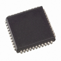
AT89LP6440-20JU Atmel, AT89LP6440-20JU Datasheet - Page 103

AT89LP6440-20JU
Manufacturer Part Number
AT89LP6440-20JU
Description
MCU 8051 64K FLASH ISP 44PLCC
Manufacturer
Atmel
Series
89LPr
Datasheet
1.AT89LP6440-20MU.pdf
(194 pages)
Specifications of AT89LP6440-20JU
Core Processor
8051
Core Size
8-Bit
Speed
20MHz
Connectivity
I²C, SPI, UART/USART
Peripherals
Brown-out Detect/Reset, POR, PWM, WDT
Number Of I /o
38
Program Memory Size
64KB (64K x 8)
Program Memory Type
FLASH
Eeprom Size
8K x 8
Ram Size
4.25K x 8
Voltage - Supply (vcc/vdd)
2.4 V ~ 3.6 V
Data Converters
A/D 8x10b
Oscillator Type
Internal
Operating Temperature
-40°C ~ 85°C
Package / Case
44-PLCC
Processor Series
AT89x
Core
8051
Data Bus Width
8 bit
Data Ram Size
8 KB
Interface Type
2-Wire, SPI
Maximum Clock Frequency
24 MHz
Number Of Programmable I/os
38
Number Of Timers
3
Operating Supply Voltage
2.7 V to 3.6 V
Maximum Operating Temperature
+ 85 C
Mounting Style
SMD/SMT
3rd Party Development Tools
PK51, CA51, A51, ULINK2
Development Tools By Supplier
AT89ISP
Minimum Operating Temperature
- 40 C
On-chip Adc
10 bit, 8 Channel
On-chip Dac
10 bit, 8 Channel
Lead Free Status / RoHS Status
Lead free / RoHS Compliant
Available stocks
Company
Part Number
Manufacturer
Quantity
Price
Company:
Part Number:
AT89LP6440-20JU
Manufacturer:
Atmel
Quantity:
103
17.4
Figure 17-3. SPI Transfer Format with CPHA = 0
Note:
Figure 17-4. SPI Transfer Format with CPHA = 1
Note:
3706A–MICRO–9/09
SSIG
DISSO
ENH
Serial Clock Timing
*Not defined but normally MSB of character just received.
(FOR REFERENCE)
*Not defined but normally LSB of previously transmitted character.
(FROM MASTER)
SCK (CPOL = 0)
SCK (CPOL = 1)
SS (TO SLAVE)
(FROM SLAVE)
Slave Select Ignore. If SSIG = 0, the SPI will only operate in slave mode if SS (P1.4) is pulled low. When SSIG = 1, the
SPI ignores SS in slave mode and is active whenever SPE (SPCR.6) is set. When MSTR = 1 and SSIG = 0, SS is
monitored for master mode collisions. Setting SSIG = 1 will ignore collisions on SS. P1.4 may be used as a regular I/O
pin when SSIG = 1.
Disable slave output bit. When set, this bit causes the MISO pin to be tristated so that more than one slave device can
share the same interface without multiple SS lines. Normally, the first byte in a transmission could be the slave address
and only the selected slave should clear its DISSO bit.
TX Buffer Interrupt Enable. When ENH = 1, TXE will generate an SPI interrupt if ESP = 1. When ENH = 0, TXE does not
generate an interrupt.
SCK CYCLE #
MOSI
MISO
The CPHA, CPOL and SPR bits in SPCR control the shape and rate of SCK. The two SPR bits
provide four possible clock rates when the SPI is in master mode. In slave mode, the SPI will
operate at the rate of the incoming SCK as long as it does not exceed the maximum bit rate.
There are also four possible combinations of SCK phase and polarity with respect to the serial
data. CPHA and CPOL determine which format is used for transmission. The SPI data transfer
formats are shown in
interface, CPHA, CPOL, and SPR should not be modified while the interface is enabled, and the
master device should be enabled before the slave device(s).
*
MSB
MSB
1
Figures 17-3 and
2
6
6
3
5
5
4
4
4
17-4. To prevent glitches on SCK from disrupting the
AT89LP6440 - Preliminary
5
3
3
6
2
2
7
1
1
8
LSB
LSB
103


