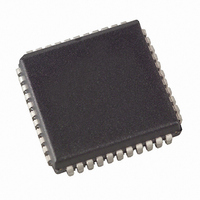
AT89LP6440-20JU Atmel, AT89LP6440-20JU Datasheet - Page 32

AT89LP6440-20JU
Manufacturer Part Number
AT89LP6440-20JU
Description
MCU 8051 64K FLASH ISP 44PLCC
Manufacturer
Atmel
Series
89LPr
Datasheet
1.AT89LP6440-20MU.pdf
(194 pages)
Specifications of AT89LP6440-20JU
Core Processor
8051
Core Size
8-Bit
Speed
20MHz
Connectivity
I²C, SPI, UART/USART
Peripherals
Brown-out Detect/Reset, POR, PWM, WDT
Number Of I /o
38
Program Memory Size
64KB (64K x 8)
Program Memory Type
FLASH
Eeprom Size
8K x 8
Ram Size
4.25K x 8
Voltage - Supply (vcc/vdd)
2.4 V ~ 3.6 V
Data Converters
A/D 8x10b
Oscillator Type
Internal
Operating Temperature
-40°C ~ 85°C
Package / Case
44-PLCC
Processor Series
AT89x
Core
8051
Data Bus Width
8 bit
Data Ram Size
8 KB
Interface Type
2-Wire, SPI
Maximum Clock Frequency
24 MHz
Number Of Programmable I/os
38
Number Of Timers
3
Operating Supply Voltage
2.7 V to 3.6 V
Maximum Operating Temperature
+ 85 C
Mounting Style
SMD/SMT
3rd Party Development Tools
PK51, CA51, A51, ULINK2
Development Tools By Supplier
AT89ISP
Minimum Operating Temperature
- 40 C
On-chip Adc
10 bit, 8 Channel
On-chip Dac
10 bit, 8 Channel
Lead Free Status / RoHS Status
Lead free / RoHS Compliant
Available stocks
Company
Part Number
Manufacturer
Quantity
Price
Company:
Part Number:
AT89LP6440-20JU
Manufacturer:
Atmel
Quantity:
103
Table 6-2.
7. Reset
7.1
32
TPS[3-0]
CDV[2-0]
COE
Symbol
CLKREG = 8FH
Not Bit Addressable
Bit
Power-on Reset
AT89LP6440 - Preliminary
Function
Timer Prescaler. The Timer Prescaler selects the time base for Timer 0, Timer 1, Timer 2 and the Watchdog Timer. The
prescaler is implemented as a 4-bit binary down counter. When the counter reaches zero it is reloaded with the value
stored in the TPS bits to give a division ratio between 1 and 16. By default the timers will count every clock cycle (TPS =
0000B). To configure the timers to count at a standard 8051 rate of once every 12 clock cycles, TPS should be set to
1011B.
System Clock Division. Determines the frequency of the system clock relative to the oscillator clock source.
CDIV2
0
0
0
0
1
1
1
1
Clock Out Enable. Set COE to output the system clock divided by 2 on XTAL2 (P4.1). The internal RC oscillator or
external clock source must be selected in order to use this feature and P4.1 must be configured as an output.
CLKREG
TPS3
7
– Clock Control Register
CDIV1
0
0
1
1
0
0
1
1
ing normal execution. Changes to CDV are synchronized such that the system clock will not
pass through intermediate frequencies. When CDV is updated, the new frequency will take
affect within a maximum period of 128 x t
During reset, all I/O Registers are set to their initial values, the port pins are tristated, and the
program starts execution from the Reset Vector, 0000H. The AT89LP6440 has five sources of
reset: power-on reset, brown-out reset, external reset, watchdog reset, and software reset.
A Power-on Reset (POR) is generated by an on-chip detection circuit. The detection level V
is nominally 1.4V. The POR is activated whenever V
cuit can be used to trigger the start-up reset or to detect a supply voltage failure in devices
without a brown-out detector. The POR circuit ensures that the device is reset from power-on. A
power-on sequence is shown in
threshold voltage V
sequence completes, the start-up timer determines how long the device is kept in POR after V
rise. The POR signal is activated again, without any delay, when V
threshold level. A Power-on Reset (i.e. a cold reset) will set the POF flag in PCON. The internally
TPS2
6
CDIV0
0
1
0
1
0
1
0
1
TPS1
5
System Clock Frequency
f
f
f
f
f
f
f
f
OSC
OSC
OSC
OSC
OSC
OSC
OSC
OSC
POR
/1
/2
/4
/8
/16
/32
/64
/128
, an initialization sequence lasting t
TPS0
4
Figure 7-1 on page
OSC
CDV2
3
.
DD
33. When V
CDV1
is below the detection level. The POR cir-
2
POR
is started. When the initialization
DD
Reset Value = 0000 0000B
reaches the Power-on Reset
CDV0
1
DD
falls below the POR
3706A–MICRO–9/09
COE
0
POR
DD


