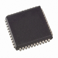
AT89LP6440-20JU Atmel, AT89LP6440-20JU Datasheet - Page 36

AT89LP6440-20JU
Manufacturer Part Number
AT89LP6440-20JU
Description
MCU 8051 64K FLASH ISP 44PLCC
Manufacturer
Atmel
Series
89LPr
Datasheet
1.AT89LP6440-20MU.pdf
(194 pages)
Specifications of AT89LP6440-20JU
Core Processor
8051
Core Size
8-Bit
Speed
20MHz
Connectivity
I²C, SPI, UART/USART
Peripherals
Brown-out Detect/Reset, POR, PWM, WDT
Number Of I /o
38
Program Memory Size
64KB (64K x 8)
Program Memory Type
FLASH
Eeprom Size
8K x 8
Ram Size
4.25K x 8
Voltage - Supply (vcc/vdd)
2.4 V ~ 3.6 V
Data Converters
A/D 8x10b
Oscillator Type
Internal
Operating Temperature
-40°C ~ 85°C
Package / Case
44-PLCC
Processor Series
AT89x
Core
8051
Data Bus Width
8 bit
Data Ram Size
8 KB
Interface Type
2-Wire, SPI
Maximum Clock Frequency
24 MHz
Number Of Programmable I/os
38
Number Of Timers
3
Operating Supply Voltage
2.7 V to 3.6 V
Maximum Operating Temperature
+ 85 C
Mounting Style
SMD/SMT
3rd Party Development Tools
PK51, CA51, A51, ULINK2
Development Tools By Supplier
AT89ISP
Minimum Operating Temperature
- 40 C
On-chip Adc
10 bit, 8 Channel
On-chip Dac
10 bit, 8 Channel
Lead Free Status / RoHS Status
Lead free / RoHS Compliant
Available stocks
Company
Part Number
Manufacturer
Quantity
Price
Company:
Part Number:
AT89LP6440-20JU
Manufacturer:
Atmel
Quantity:
103
Table 8-1.
8.2
8.2.1
36
Symbol
SMOD1
SMOD0
PWDEX
POF
GF1, GF0
PD
IDL
PCON = 87H
Not Bit Addressable
Bit
Power-down Mode
AT89LP6440 - Preliminary
Interrupt Recovery from Power-down
Function
Double Baud Rate bit. Doubles the baud rate of the UART in Modes 1, 2, or 3.
Frame Error Select. When SMOD0 = 1, SCON.7 is SM0. When SMOD0 = 1, SCON.7 is FE. Note that FE will be set after
a frame error regardless of the state of SMOD0.
Power-down Exit Mode. When PWDEX = 1, wake up from Power-down is externally controlled. When PWDEX = 1, wake
up from Power-down is internally timed.
Power Off Flag. POF is set to “1” during power up (i.e. cold reset). It can be set or reset under software control and is not
affected by RST or BOD (i.e. warm resets).
General-purpose Flags
Power-down bit. Setting this bit activates power-down operation. The PD bit is cleared automatically by hardware when
waking up from power-down.
Idle Mode bit. Setting this bit activates Idle mode operation. The IDL bit is cleared automatically by hardware when
waking up from idle
PCON
SMOD1
7
– Power Control Register
.
Setting the Power-down (PD) bit in PCON enters Power-down mode. Power-down mode stops
the oscillator, disables the BOD and powers down the Flash memory in order to minimize power
consumption. Only the power-on circuitry will continue to draw power during Power-down. Dur-
ing Power-down, the power supply voltage may be reduced to the RAM keep-alive voltage. The
RAM contents will be retained, but the SFR contents are not guaranteed once V
reduced. Power-down may be exited by external reset, power-on reset, or certain enabled
interrupts.
Three external interrupt sources may be configured to terminate Power-down mode: external
interrupts INT0 (P3.2) and INT1 (P3.3); and the general-purpose interrupts (GPI). To wake up by
external interrupt INT0 or INT1, that interrupt must be enabled by setting EX0 or EX1 in IE and
must be configured for level-sensitive operation by clearing IT0 or IT1. Any General-purpose
interrupt on Port 1 (GPI
and configured for level-sensitive detection, and EGP in IE2 must be set in order to terminate
Power-down.
When terminating Power-down by an interrupt, two different wake-up modes are available.
When PWDEX in PCON is zero, the wake-up period is internally timed as shown in
At the falling edge on the interrupt pin, Power-down is exited, the oscillator is restarted, and an
internal timer begins counting. The internal clock will not be allowed to propagate to the CPU
until after the timer has timed out. After the time-out period the interrupt service routine will
begin. The time-out period is controlled by the Start-up Timer Fuses (see
The interrupt pin need not remain low for the entire time-out period.
SMOD0
6
PWDEX
5
7-0
) can also wake up the device. The GPI pin must be enabled in GPIEN
POF
4
GF1
3
GF0
2
Reset Value = 000X 0000B
PD
1
Table 7-1 on page
3706A–MICRO–9/09
IDL
0
DD
Figure
has been
8-1.
34).


