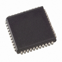
AT89LP6440-20JU Atmel, AT89LP6440-20JU Datasheet - Page 123

AT89LP6440-20JU
Manufacturer Part Number
AT89LP6440-20JU
Description
MCU 8051 64K FLASH ISP 44PLCC
Manufacturer
Atmel
Series
89LPr
Datasheet
1.AT89LP6440-20MU.pdf
(194 pages)
Specifications of AT89LP6440-20JU
Core Processor
8051
Core Size
8-Bit
Speed
20MHz
Connectivity
I²C, SPI, UART/USART
Peripherals
Brown-out Detect/Reset, POR, PWM, WDT
Number Of I /o
38
Program Memory Size
64KB (64K x 8)
Program Memory Type
FLASH
Eeprom Size
8K x 8
Ram Size
4.25K x 8
Voltage - Supply (vcc/vdd)
2.4 V ~ 3.6 V
Data Converters
A/D 8x10b
Oscillator Type
Internal
Operating Temperature
-40°C ~ 85°C
Package / Case
44-PLCC
Processor Series
AT89x
Core
8051
Data Bus Width
8 bit
Data Ram Size
8 KB
Interface Type
2-Wire, SPI
Maximum Clock Frequency
24 MHz
Number Of Programmable I/os
38
Number Of Timers
3
Operating Supply Voltage
2.7 V to 3.6 V
Maximum Operating Temperature
+ 85 C
Mounting Style
SMD/SMT
3rd Party Development Tools
PK51, CA51, A51, ULINK2
Development Tools By Supplier
AT89ISP
Minimum Operating Temperature
- 40 C
On-chip Adc
10 bit, 8 Channel
On-chip Dac
10 bit, 8 Channel
Lead Free Status / RoHS Status
Lead free / RoHS Compliant
Available stocks
Company
Part Number
Manufacturer
Quantity
Price
Company:
Part Number:
AT89LP6440-20JU
Manufacturer:
Atmel
Quantity:
103
18.6.4
Figure 18-14. Format and States in Slave Transmitter Mode
3706A–MICRO–9/09
Reception of the own
slave address and one or
more data bytes
Arbitration lost as master
and addressed as slave
Last data byte transmitted.
Switched to not addressed
slave (TWEA = '0')
Slave Transmitter Mode
From master to slave
From slave to master
In the Slave Transmitter mode, a number of data bytes are transmitted to a master receiver. To
initiate the Slave Transmitter mode, upper 7 bits of TWAR must be initialized with the address to
which the Two-wire Serial Interface will respond when addressed by a master. If the LSB is set,
the TWI will respond to the general call address (00h), otherwise it will ignore the general call
address. TWEN must be written to one to enable the TWI. The AA bit must be written to one to
enable the acknowledgment of the device’s own slave address or the general call address. STA
and STO must be written to zero.
When TWAR and TWCR have been initialized, the TWI waits until it is addressed by its own
slave address (or the general call address if enabled) followed by the data direction bit. If the
direction bit is “1” (read), the TWI will operate in ST mode, otherwise SR mode is entered. After
its own slave address and the write bit have been received, the TWINT flag is set and a valid
status code can be read from TWSR. The status code is used to determine the appropriate soft-
ware action. The appropriate action to be taken for each status code is detailed in
The Slave Transmitter mode may also be entered if arbitration is lost while the TWI is in the
Master mode (see state B0h).
If the AA bit is written to zero during a transfer, the TWI will transmit the last byte of the transfer.
State C0h or state C8h will be entered, depending on whether the master receiver transmits a
NACK or ACK after the final byte. The TWI is switched to the not addressed Slave mode, and
will ignore the master if it continues the transfer. Thus the master receiver receives all “1s” as
serial data. State C8h is entered if the master demands additional data bytes (by transmitting
ACK), even though the slave has transmitted the last byte (AA zero and expecting NACK from
the master). While AA is zero, the TWI does not respond to its own slave address. However, the
Two-wire Serial Bus is still monitored and address recognition may resume at any time by set-
ting AA. This implies that the AA bit may be used to temporarily isolate the TWI from the Two-
wire Serial Bus.
S
SLA
R
DATA
A8h
B0h
A
A
n
A
DATA
Any number of data bytes
and their associated acknowledge bits
This number (contained in TWSR) corresponds
to a defined state of the Two-wire Serial Bus. The
prescaler bits are zero or masked to zero
AT89LP6440 - Preliminary
B8h
A
DATA
C0h
C8h
A
A
P or S
All 1's
Table
P or S
18-9.
123


