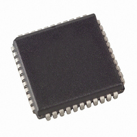
AT89LP6440-20JU Atmel, AT89LP6440-20JU Datasheet - Page 98

AT89LP6440-20JU
Manufacturer Part Number
AT89LP6440-20JU
Description
MCU 8051 64K FLASH ISP 44PLCC
Manufacturer
Atmel
Series
89LPr
Datasheet
1.AT89LP6440-20MU.pdf
(194 pages)
Specifications of AT89LP6440-20JU
Core Processor
8051
Core Size
8-Bit
Speed
20MHz
Connectivity
I²C, SPI, UART/USART
Peripherals
Brown-out Detect/Reset, POR, PWM, WDT
Number Of I /o
38
Program Memory Size
64KB (64K x 8)
Program Memory Type
FLASH
Eeprom Size
8K x 8
Ram Size
4.25K x 8
Voltage - Supply (vcc/vdd)
2.4 V ~ 3.6 V
Data Converters
A/D 8x10b
Oscillator Type
Internal
Operating Temperature
-40°C ~ 85°C
Package / Case
44-PLCC
Processor Series
AT89x
Core
8051
Data Bus Width
8 bit
Data Ram Size
8 KB
Interface Type
2-Wire, SPI
Maximum Clock Frequency
24 MHz
Number Of Programmable I/os
38
Number Of Timers
3
Operating Supply Voltage
2.7 V to 3.6 V
Maximum Operating Temperature
+ 85 C
Mounting Style
SMD/SMT
3rd Party Development Tools
PK51, CA51, A51, ULINK2
Development Tools By Supplier
AT89ISP
Minimum Operating Temperature
- 40 C
On-chip Adc
10 bit, 8 Channel
On-chip Dac
10 bit, 8 Channel
Lead Free Status / RoHS Status
Lead free / RoHS Compliant
Available stocks
Company
Part Number
Manufacturer
Quantity
Price
Company:
Part Number:
AT89LP6440-20JU
Manufacturer:
Atmel
Quantity:
103
98
AT89LP6440 - Preliminary
Figure 17-1. SPI Block Diagram
The interconnection between master and slave CPUs with SPI is shown in
pins in the interface are Master-In/Slave-Out (MISO), Master-Out/Slave-In (MOSI), Shift Clock
(SCK), and Slave Select (SS). The SCK pin is the clock output in master mode, but is the clock
input in slave mode. The MSTR bit in SPCR determines the directions of MISO and MOSI. Also
notice that MOSI connects to MOSI and MISO to MISO. By default SS/P1.4 is an input to both
master and slave devices.
In slave mode, SS must be driven low to select an individual device as a slave. When SS is held
low, the SPI is activated, and MISO becomes an output if configured so by the user. All other
pins are inputs. When SS is driven high, all pins are inputs, and the SPI is passive, which means
that it will not receive incoming data. Note that the SPI logic will be reset once the SS pin is
driven high. The SS pin is useful for packet/byte synchronization to keep the slave bit counter
synchronous with the master clock generator. When the SS pin is driven high, the SPI slave will
immediately reset the send and receive logic, and drop any partially received data in the Shift
Register.The slave may ignore SS by setting its SSIG bit in SPSR. When SSIG = 1, the slave is
always enabled and operates in 3-wire mode. However, the slave output on MISO may still be
disabled by setting DISSO = 1.
T1 OVF
÷4/÷8/÷32/÷64
SPI Status Register
Oscillator
Select
Divider
1
0
SPI Control
TSCK
SPI Clock (Master)
SPI Interrupt
Request
MSTR
SPE
8
MSB
Data Bus
Internal
8
Read Data Buffer
Write Data Buffer
8-bit Shift Register
8
SPI Control Register
Clock
Logic
LSB
Figure
S
M
M
S
S
M
3706A–MICRO–9/09
17-2. The four
MISO
MOSI
P1.6
P1.5
SCK
P1.4
1.7
SS


