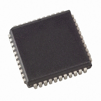
AT89LP6440-20JU Atmel, AT89LP6440-20JU Datasheet - Page 47

AT89LP6440-20JU
Manufacturer Part Number
AT89LP6440-20JU
Description
MCU 8051 64K FLASH ISP 44PLCC
Manufacturer
Atmel
Series
89LPr
Datasheet
1.AT89LP6440-20MU.pdf
(194 pages)
Specifications of AT89LP6440-20JU
Core Processor
8051
Core Size
8-Bit
Speed
20MHz
Connectivity
I²C, SPI, UART/USART
Peripherals
Brown-out Detect/Reset, POR, PWM, WDT
Number Of I /o
38
Program Memory Size
64KB (64K x 8)
Program Memory Type
FLASH
Eeprom Size
8K x 8
Ram Size
4.25K x 8
Voltage - Supply (vcc/vdd)
2.4 V ~ 3.6 V
Data Converters
A/D 8x10b
Oscillator Type
Internal
Operating Temperature
-40°C ~ 85°C
Package / Case
44-PLCC
Processor Series
AT89x
Core
8051
Data Bus Width
8 bit
Data Ram Size
8 KB
Interface Type
2-Wire, SPI
Maximum Clock Frequency
24 MHz
Number Of Programmable I/os
38
Number Of Timers
3
Operating Supply Voltage
2.7 V to 3.6 V
Maximum Operating Temperature
+ 85 C
Mounting Style
SMD/SMT
3rd Party Development Tools
PK51, CA51, A51, ULINK2
Development Tools By Supplier
AT89ISP
Minimum Operating Temperature
- 40 C
On-chip Adc
10 bit, 8 Channel
On-chip Dac
10 bit, 8 Channel
Lead Free Status / RoHS Status
Lead free / RoHS Compliant
Available stocks
Company
Part Number
Manufacturer
Quantity
Price
Company:
Part Number:
AT89LP6440-20JU
Manufacturer:
Atmel
Quantity:
103
10.2
10.3
3706A–MICRO–9/09
Port Analog Functions
Port Read-Modify-Write
The AT89LP6440 incorporates two analog comparators and an 8-channel analog-to-digital con-
verter. In order to give the best analog performance and minimize power consumption, pins that
are being used for analog functions must have both their digital outputs and digital inputs dis-
abled. Digital outputs are disabled by putting the port pins into the input-only mode as described
in
after reset regardless of the state of the Tristate-Port Fuse.
Digital inputs on P2.4, P2.5, P2.6 and P2.7 are disabled whenever an analog comparator is
enabled by setting the CENA or CENB bits in ACSRA and ACSRB and that pin is configured for
input-only mode. To use an analog input pin as a high-impedance digital input while a compara-
tor is enabled, that pin should be configured in open-drain mode and the corresponding port
register bit should be set to 1.
Digital inputs on Port 0 are disabled for each pin configured for input-only mode whenever the
ADC is enabled by setting the ADCE bit and clearing the DAC bit in DADC. To use any Port 0
input pin as a high-impedance digital input while the ADC is enabled, that pin should be config-
ured in open-drain mode and the corresponding port register bit should be set to 1. When DAC
mode is enabled, P2.2 and P2.3 are forced to input-only mode.
A read from a port will read either the state of the pins or the state of the port register depending
on which instruction is used. Simple read instructions will always access the port pins directly.
Read-modify-write instructions, which read a value, possibly modify it, and then write it back, will
always access the port register. This includes bit write instructions such as CLR or SETB as they
actually read the entire port, modify a single bit, then write the data back to the entire port. See
Table 10-4
Table 10-4.
Mnemonic
ANL
ORL
XRL
JBC
CPL
INC
DEC
DJNZ
MOV PX.Y, C
CLR PX.Y
SETB PX.Y
“Port Configuration” on page
for a complete list of Read-Modify-Write instruction which may access the ports.
Port Read-Modify-Write Instructions
Instruction
Logical AND
Logical OR
Logical EX-OR
Jump if bit set and clear bit
Complement bit
Increment
Decrement
Decrement and jump if not zero
Move carry to bit Y of Port X
Clear bit Y of Port X
Set bit Y of Port X
44. The analog input pins will always default to input-only mode
AT89LP6440 - Preliminary
Example
ANL P1, A
ORL P1, A
XRL P1, A
JBC P3.0, LABEL
CPL P3.1
INC P1
DEC P3
DJNZ P3, LABEL
MOV P1.0, C
CLR P1.1
SETB P3.2
47


