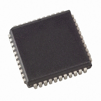
AT89LP6440-20JU Atmel, AT89LP6440-20JU Datasheet - Page 84

AT89LP6440-20JU
Manufacturer Part Number
AT89LP6440-20JU
Description
MCU 8051 64K FLASH ISP 44PLCC
Manufacturer
Atmel
Series
89LPr
Datasheet
1.AT89LP6440-20MU.pdf
(194 pages)
Specifications of AT89LP6440-20JU
Core Processor
8051
Core Size
8-Bit
Speed
20MHz
Connectivity
I²C, SPI, UART/USART
Peripherals
Brown-out Detect/Reset, POR, PWM, WDT
Number Of I /o
38
Program Memory Size
64KB (64K x 8)
Program Memory Type
FLASH
Eeprom Size
8K x 8
Ram Size
4.25K x 8
Voltage - Supply (vcc/vdd)
2.4 V ~ 3.6 V
Data Converters
A/D 8x10b
Oscillator Type
Internal
Operating Temperature
-40°C ~ 85°C
Package / Case
44-PLCC
Processor Series
AT89x
Core
8051
Data Bus Width
8 bit
Data Ram Size
8 KB
Interface Type
2-Wire, SPI
Maximum Clock Frequency
24 MHz
Number Of Programmable I/os
38
Number Of Timers
3
Operating Supply Voltage
2.7 V to 3.6 V
Maximum Operating Temperature
+ 85 C
Mounting Style
SMD/SMT
3rd Party Development Tools
PK51, CA51, A51, ULINK2
Development Tools By Supplier
AT89ISP
Minimum Operating Temperature
- 40 C
On-chip Adc
10 bit, 8 Channel
On-chip Dac
10 bit, 8 Channel
Lead Free Status / RoHS Status
Lead free / RoHS Compliant
Available stocks
Company
Part Number
Manufacturer
Quantity
Price
Company:
Part Number:
AT89LP6440-20JU
Manufacturer:
Atmel
Quantity:
103
16. Serial Interface (UART)
16.1
84
Multiprocessor Communications
AT89LP6440 - Preliminary
The serial interface on the AT89LP6440 implements a Universal Asynchronous Receiver/Trans-
mitter (UART). The UART has the following features:
The serial interface is full-duplex, which means it can transmit and receive simultaneously. It is
also receive-buffered, which means it can begin receiving a second byte before a previously
received byte has been read from the receive register. (However, if the first byte still has not
been read when reception of the second byte is complete, one of the bytes will be lost.) The
serial port receive and transmit registers are both accessed at the Special Function Register
SBUF. Writing to SBUF loads the transmit register, and reading SBUF accesses a physically
separate receive register. The serial port can operate in the following four modes.
In all four modes, transmission is initiated by any instruction that uses SBUF as a destination
register. Reception is initiated in Mode 0 by the condition RI = 0 and REN = 1. Reception is initi-
ated in the other modes by the incoming start bit if REN = 1.
Modes 2 and 3 have a special provision for multiprocessor communications. In these modes,
9 data bits are received, followed by a stop bit. The 9th bit goes into RB8. Then comes a stop bit.
The port can be programmed such that when the stop bit is received, the serial port interrupt is
activated only if RB8 = 1. This feature is enabled by setting bit SM2 in SCON.
The following example shows how to use the serial interrupt for multiprocessor communications.
When the master processor must transmit a block of data to one of several slaves, it first sends
out an address byte that identifies the target slave. An address byte differs from a data byte in
that the 9th bit is “1” in an address byte and “0” in a data byte. With SM2 = 1, no slave is
interrupted by a data byte. An address byte, however, interrupts all slaves. Each slave can
examine the received byte and see if it is being addressed. The addressed slave clears its SM2
• Full-duplex Operation
• 8 or 9 Data Bits
• Framing Error Detection
• Multiprocessor Communication Mode with Automatic Address Recognition
• Baud Rate Generator Using Timer 1 or Timer 2
• Interrupt on Receive Buffer Full or Transmission Complete
• Mode 0: Serial data enters and exits through RXD. TXD outputs the shift clock. Eight data
• Mode 1: 10 bits are transmitted (through TXD) or received (through RXD): a start bit (0),
• Mode 2: 11 bits are transmitted (through TXD) or received (through RXD): a start bit (0),
• Mode 3: 11 bits are transmitted (through TXD) or received (through RXD): a start bit (0),
bits are transmitted/received, with the LSB first. The baud rate is programmable to 1/2 or 1/4
the oscillator frequency, or variable based on Time 1.
8 data bits (LSB first), and a stop bit (1). On receive, the stop bit goes into RB8 in the Special
Function Register SCON. The baud rate is variable based on Timer 1 or Timer 2.
8 data bits (LSB first), a programmable 9th data bit, and a stop bit (1). On transmit, the 9th
data bit (TB8 in SCON) can be assigned the value of “0” or “1”. For example, the parity bit
(P, in the PSW) can be moved into TB8. On receive, the 9th data bit goes into RB8 in the
Special Function Register SCON, while the stop bit is ignored. The baud rate is
programmable to either 1/16 or 1/32 the oscillator frequency.
8 data bits (LSB first), a programmable 9th data bit, and a stop bit (1). In fact, Mode 3 is the
same as Mode 2 in all respects except the baud rate, which is variable based on Timer 1 or
Timer 3 in Mode 3.
3706A–MICRO–9/09


