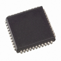
AT89LP6440-20JU Atmel, AT89LP6440-20JU Datasheet - Page 79

AT89LP6440-20JU
Manufacturer Part Number
AT89LP6440-20JU
Description
MCU 8051 64K FLASH ISP 44PLCC
Manufacturer
Atmel
Series
89LPr
Datasheet
1.AT89LP6440-20MU.pdf
(194 pages)
Specifications of AT89LP6440-20JU
Core Processor
8051
Core Size
8-Bit
Speed
20MHz
Connectivity
I²C, SPI, UART/USART
Peripherals
Brown-out Detect/Reset, POR, PWM, WDT
Number Of I /o
38
Program Memory Size
64KB (64K x 8)
Program Memory Type
FLASH
Eeprom Size
8K x 8
Ram Size
4.25K x 8
Voltage - Supply (vcc/vdd)
2.4 V ~ 3.6 V
Data Converters
A/D 8x10b
Oscillator Type
Internal
Operating Temperature
-40°C ~ 85°C
Package / Case
44-PLCC
Processor Series
AT89x
Core
8051
Data Bus Width
8 bit
Data Ram Size
8 KB
Interface Type
2-Wire, SPI
Maximum Clock Frequency
24 MHz
Number Of Programmable I/os
38
Number Of Timers
3
Operating Supply Voltage
2.7 V to 3.6 V
Maximum Operating Temperature
+ 85 C
Mounting Style
SMD/SMT
3rd Party Development Tools
PK51, CA51, A51, ULINK2
Development Tools By Supplier
AT89ISP
Minimum Operating Temperature
- 40 C
On-chip Adc
10 bit, 8 Channel
On-chip Dac
10 bit, 8 Channel
Lead Free Status / RoHS Status
Lead free / RoHS Compliant
Available stocks
Company
Part Number
Manufacturer
Quantity
Price
Company:
Part Number:
AT89LP6440-20JU
Manufacturer:
Atmel
Quantity:
103
- Current page: 79 of 194
- Download datasheet (6Mb)
Figure 13-10. Phase and Frequency Correct Symmetrical (Center-Aligned) PWM
Figure 13-11. Phase Correct Symmetrical (Center-Aligned) PWM
13.4.3
3706A–MICRO–9/09
Multi-Phasic PWM
{RCAP2H,RCA2L}
{RCAP2H,RCA2L}
{CCxH,CCxL}
{CCxH,CCxL}
Non-Inverted
Non-Inverted
Inverted
Inverted
CCx
CCx
The PWM channels may be configured to provide multi-phasic alternating outputs by the PHS
bits in T2MOD. The AT89LP6440 provides 1 out of 2, 1 out of 3, 1 out of 4 and 2 out of 4 phase
modes (See
are connected to a one-hot shift register that selectively enables and disables the outputs (See
Figure
the compare value was set equal to TOP. The PHSD bit in T2MOD controls the direction of the
shift register. Example waveforms are shown in
phasic PWM, the associated channels must be configured for PWM operation. Non-PWM chan-
nels are not affected by multi-phasic operation. However, their locations in the shift register are
maintained such that some periods in the PWM outputs may not have any pulses as shown in
Figure
The PHS
PHSD are allowed at any time. Note that channels C and D in 1:2 phase mode and channel D in
1:3 phase mode operate normally.
13-13.
13-12). Compare points on disabled channels are blocked from toggling the output as if
2-0
bits may only be modified when the timer is not operational (TR2 = 0). Updates to
Table
13-6). In Multi-phasic mode the PWM outputs on CCA, CCB, CCC and CCD
CP/RL2 = 0, T2CM
CP/RL2 = 0, T2CM
1-0
1-0
= 11B, DCEN = 0
= 10B, DCEN = 0
AT89LP6440 - Preliminary
Figure 13-14 on page
Duty Cycle Updated
Duty Cycle Updated
81. In order to use multi-
79
2-0
Related parts for AT89LP6440-20JU
Image
Part Number
Description
Manufacturer
Datasheet
Request
R

Part Number:
Description:
DEV KIT FOR AVR/AVR32
Manufacturer:
Atmel
Datasheet:

Part Number:
Description:
INTERVAL AND WIPE/WASH WIPER CONTROL IC WITH DELAY
Manufacturer:
ATMEL Corporation
Datasheet:

Part Number:
Description:
Low-Voltage Voice-Switched IC for Hands-Free Operation
Manufacturer:
ATMEL Corporation
Datasheet:

Part Number:
Description:
MONOLITHIC INTEGRATED FEATUREPHONE CIRCUIT
Manufacturer:
ATMEL Corporation
Datasheet:

Part Number:
Description:
AM-FM Receiver IC U4255BM-M
Manufacturer:
ATMEL Corporation
Datasheet:

Part Number:
Description:
Monolithic Integrated Feature Phone Circuit
Manufacturer:
ATMEL Corporation
Datasheet:

Part Number:
Description:
Multistandard Video-IF and Quasi Parallel Sound Processing
Manufacturer:
ATMEL Corporation
Datasheet:

Part Number:
Description:
High-performance EE PLD
Manufacturer:
ATMEL Corporation
Datasheet:

Part Number:
Description:
8-bit Flash Microcontroller
Manufacturer:
ATMEL Corporation
Datasheet:

Part Number:
Description:
2-Wire Serial EEPROM
Manufacturer:
ATMEL Corporation
Datasheet:


