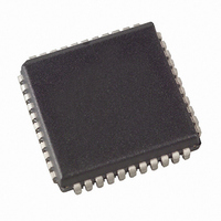
AT89LP6440-20JU Atmel, AT89LP6440-20JU Datasheet - Page 12

AT89LP6440-20JU
Manufacturer Part Number
AT89LP6440-20JU
Description
MCU 8051 64K FLASH ISP 44PLCC
Manufacturer
Atmel
Series
89LPr
Datasheet
1.AT89LP6440-20MU.pdf
(194 pages)
Specifications of AT89LP6440-20JU
Core Processor
8051
Core Size
8-Bit
Speed
20MHz
Connectivity
I²C, SPI, UART/USART
Peripherals
Brown-out Detect/Reset, POR, PWM, WDT
Number Of I /o
38
Program Memory Size
64KB (64K x 8)
Program Memory Type
FLASH
Eeprom Size
8K x 8
Ram Size
4.25K x 8
Voltage - Supply (vcc/vdd)
2.4 V ~ 3.6 V
Data Converters
A/D 8x10b
Oscillator Type
Internal
Operating Temperature
-40°C ~ 85°C
Package / Case
44-PLCC
Processor Series
AT89x
Core
8051
Data Bus Width
8 bit
Data Ram Size
8 KB
Interface Type
2-Wire, SPI
Maximum Clock Frequency
24 MHz
Number Of Programmable I/os
38
Number Of Timers
3
Operating Supply Voltage
2.7 V to 3.6 V
Maximum Operating Temperature
+ 85 C
Mounting Style
SMD/SMT
3rd Party Development Tools
PK51, CA51, A51, ULINK2
Development Tools By Supplier
AT89ISP
Minimum Operating Temperature
- 40 C
On-chip Adc
10 bit, 8 Channel
On-chip Dac
10 bit, 8 Channel
Lead Free Status / RoHS Status
Lead free / RoHS Compliant
Available stocks
Company
Part Number
Manufacturer
Quantity
Price
Company:
Part Number:
AT89LP6440-20JU
Manufacturer:
Atmel
Quantity:
103
3.2.2
3.2.3
3.3
3.3.1
12
External Data Memory
AT89LP6440 - Preliminary
IDATA
SFR
XDATA
The full 256 byte internal RAM can be indirectly addressed using the 8-bit pointers R0 and R1.
The first 128 bytes of IDATA include the DATA space. The hardware stack is also located in the
IDATA space when XSTK = 0.
The upper 128 direct addresses (80H–FFH) access the I/O registers. I/O registers on AT89LP
devices are referred to as Special Function Registers. The SFRs can only be accessed through
direct addressing. All SFR locations are not implemented. See
SFRs.
AT89LP microcontrollers support a 16-bit external memory address space for up to 64K bytes of
external data memory (XDATA). The external memory space is accessed with the MOVX
instructions. Some internal data memory resources are mapped into portions of the external
address space as shown in
the CPU can access them. The AT89LP6440 includes 4K bytes of on-chip Extra RAM (EDATA)
and 8K bytes of nonvolatile Flash data memory (FDATA).
Figure 3-3.
The external data memory space can accommodate up to 64KB of external memory. The
AT89LP6440 uses the standard 8051 external memory interface with the upper address byte on
Port 2, the lower address byte and data in/out multiplexed on Port 0, and the ALE, RD and WR
strobes. MOVX instructions targeted to XDATA require a minimum of 4 clock cycles. XDATA can
be accessed with both 16-bit (MOVX @DPTR) and 8-bit (MOVX @Ri) addresses. See
3.3.4 on page 16
0000
FFFF
(XDATA: 64KB)
External Data
External Data Memory Map
EXRAM = 1
for more details of the external memory interface.
Figure
3-3. These memory spaces may require configuration before
1000
0FFF
FFFF
(XDATA: 60KB)
External Data
(EDATA: 4KB)
EXRAM = 0
Extra RAM
DMEN = 0
Section 4.
3000
1000
2FFF
0FFF
FFFF
for a listed of available
(XDATA: 52KB)
External Data
(FDATA: 8KB)
(EDATA: 4KB)
EXRAM = 0
Flash Data
Extra RAM
DMEN = 1
3706A–MICRO–9/09
Section


