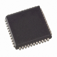
AT89LP6440-20JU Atmel, AT89LP6440-20JU Datasheet - Page 55

AT89LP6440-20JU
Manufacturer Part Number
AT89LP6440-20JU
Description
MCU 8051 64K FLASH ISP 44PLCC
Manufacturer
Atmel
Series
89LPr
Datasheet
1.AT89LP6440-20MU.pdf
(194 pages)
Specifications of AT89LP6440-20JU
Core Processor
8051
Core Size
8-Bit
Speed
20MHz
Connectivity
I²C, SPI, UART/USART
Peripherals
Brown-out Detect/Reset, POR, PWM, WDT
Number Of I /o
38
Program Memory Size
64KB (64K x 8)
Program Memory Type
FLASH
Eeprom Size
8K x 8
Ram Size
4.25K x 8
Voltage - Supply (vcc/vdd)
2.4 V ~ 3.6 V
Data Converters
A/D 8x10b
Oscillator Type
Internal
Operating Temperature
-40°C ~ 85°C
Package / Case
44-PLCC
Processor Series
AT89x
Core
8051
Data Bus Width
8 bit
Data Ram Size
8 KB
Interface Type
2-Wire, SPI
Maximum Clock Frequency
24 MHz
Number Of Programmable I/os
38
Number Of Timers
3
Operating Supply Voltage
2.7 V to 3.6 V
Maximum Operating Temperature
+ 85 C
Mounting Style
SMD/SMT
3rd Party Development Tools
PK51, CA51, A51, ULINK2
Development Tools By Supplier
AT89ISP
Minimum Operating Temperature
- 40 C
On-chip Adc
10 bit, 8 Channel
On-chip Dac
10 bit, 8 Channel
Lead Free Status / RoHS Status
Lead free / RoHS Compliant
Available stocks
Company
Part Number
Manufacturer
Quantity
Price
Company:
Part Number:
AT89LP6440-20JU
Manufacturer:
Atmel
Quantity:
103
Table 11-4.
11.5
3706A–MICRO–9/09
Symbol
PWM1EN
PWM0EN
PSC12
PSC11
PSC10
PSC02
PSC01
PSC00
TCONB = 91H
Not Bit Addressable
Bit
Pulse Width Modulation
Function
Configures Timer 1 for Pulse Width Modulation output on T1 (P3.5).
Configures Timer 0 for Pulse Width Modulation output on T0 (P3.4).
Prescaler for Timer 1 Mode 0. The number of active bits in TL1 equals PSC1 + 1. After reset PSC1 = 100B which
enables 5 bits of TL1 for compatibility with the 13-bit Mode 0 in AT89S2051.
Prescaler for Timer 0 Mode 0. The number of active bits in TL0 equals PSC0 + 1. After reset PSC0 = 100B which
enables 5 bits of TL0 for compatibility with the 13-bit Mode 0 in AT89C52.
PWM1EN
TCONB
7
– Timer/Counter Control Register B
On the AT89LP6440, Timer 0 and Timer 1 may be independently configured as 8-bit asymmetri-
cal (edge-aligned) pulse width modulators (PWM) by setting the PWM0EN or PWM1EN bits in
TCONB, respectively. In PWM Mode the generated waveform is output on the timer's input pin,
T0 or T1. Therefore, C/Tx must be set to “0” when in PWM mode and the T0 (P3.4) and T1
(P3.5) must be configured in an output mode. The Timer Overflow Flags and Interrupts will con-
tinue to function while in PWM Mode and Timer 1 may still generate the baud rate for the UART.
The timer GATE function also works in PWM mode, allowing the output to be halted by an exter-
nal input. Each PWM channel has four modes selected by the mode bits in TMOD.
An example waveform for Timer 0 in PWM Mode 0 is shown in
counter while RH0 stores the 8-bit compare value. When TH0 is 00H the PWM output is
set high. When the TH0 count reaches the value stored in RH0 the PWM output is set low.
Therefore, the pulse width is proportional to the value in RH0. To prevent glitches, writes to
RH0 only take effect on the FFH to 00H overflow of TH0. Setting RH0 to 00H will keep the PWM
output low.
Figure 11-5. 8-bit Asymmetrical Pulse Width Modulation
PWM0EN
6
(P3.4)T0
FFH
RH0
00H
TH0
PSC12
5
PSC11
4
PSC10
3
AT89LP6440 - Preliminary
TF0 Set
PSC02
2
Figure
Reset Value = 0010 0100B
PSC01
1
11-5. TH0 acts as an 8-bit
PSC00
0
time
55


