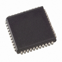
AT89LP6440-20JU Atmel, AT89LP6440-20JU Datasheet - Page 133

AT89LP6440-20JU
Manufacturer Part Number
AT89LP6440-20JU
Description
MCU 8051 64K FLASH ISP 44PLCC
Manufacturer
Atmel
Series
89LPr
Datasheet
1.AT89LP6440-20MU.pdf
(194 pages)
Specifications of AT89LP6440-20JU
Core Processor
8051
Core Size
8-Bit
Speed
20MHz
Connectivity
I²C, SPI, UART/USART
Peripherals
Brown-out Detect/Reset, POR, PWM, WDT
Number Of I /o
38
Program Memory Size
64KB (64K x 8)
Program Memory Type
FLASH
Eeprom Size
8K x 8
Ram Size
4.25K x 8
Voltage - Supply (vcc/vdd)
2.4 V ~ 3.6 V
Data Converters
A/D 8x10b
Oscillator Type
Internal
Operating Temperature
-40°C ~ 85°C
Package / Case
44-PLCC
Processor Series
AT89x
Core
8051
Data Bus Width
8 bit
Data Ram Size
8 KB
Interface Type
2-Wire, SPI
Maximum Clock Frequency
24 MHz
Number Of Programmable I/os
38
Number Of Timers
3
Operating Supply Voltage
2.7 V to 3.6 V
Maximum Operating Temperature
+ 85 C
Mounting Style
SMD/SMT
3rd Party Development Tools
PK51, CA51, A51, ULINK2
Development Tools By Supplier
AT89ISP
Minimum Operating Temperature
- 40 C
On-chip Adc
10 bit, 8 Channel
On-chip Dac
10 bit, 8 Channel
Lead Free Status / RoHS Status
Lead free / RoHS Compliant
Available stocks
Company
Part Number
Manufacturer
Quantity
Price
Company:
Part Number:
AT89LP6440-20JU
Manufacturer:
Atmel
Quantity:
103
20. Digital-to-Analog/Analog-to-Digital Converter
3706A–MICRO–9/09
The AT89LP6440 includes a 10-bit Data Converter (DADC) with the following features:
The AT89LP6440 features a 10-bit successive approximation data converter that functions in
either Analog-to-Digital (ADC) or Digital-to-Analog (DAC) mode. A block diagram of the con-
verter is shown in
four differential voltage inputs from the pins of Port 0 to a sample-and-hold circuit that in turn
provides an input to the successive approximation block. The Sample-and-Hold circuit ensures
that the input voltage to the ADC is held at a constant level during conversion. The SAR block
digitizes the analog voltage into a 10-bit value accessible through a data register. The SAR
block also operates in reverse to generate an analog voltage on Port 2 from a 10-bit digital
value. The DADC has separate analog supply pins, AV
than ± 0.3V from the standard supplies V
ADC results are available in the DADL and DADH register pair. The ADC result scale is deter-
mined by the reference voltage (V
externally from AV
form, with single-ended voltage channels referring to the level above or below AV
bit results may be right or left adjusted within the 16-bit register. The sign is extended through
the 6 MSBs of right-adjusted results and the 6 LSBs of left-adjusted results are zeroed. If only 8-
bit precision is required, the user should select left-adjusted by setting LADJ in DADC and read
only the DADH register. Example results are listed in
The conversion formulas are as follows:
Conversion results can be converted into unsigned binary by adding 02h to DADH in right-
adjusted mode or 80h to DADH in left-adjusted mode. When using the external reference
(AV
To convert the unsigned binary value back to 2’s complement, subtract 02h from DADH in right-
adjusted mode or 80h from DADH in left-adjusted mode. Note that the DADH/DADL registers
cannot be directly manipulated as they are read-only in ADC mode and write-only in DAC mode.
• Digital-to-Analog (DAC) or Analog-to-Digital (ADC) Mode
• 10-bit Resolution
• 6.5 µs Conversion Time
• 8 Multiplexed Single-ended Channels or 4 Differential Channels
• Selectable 1.0V±10% Internal Reference Voltage
• Optional Left-Adjust of Conversion Results
• Single Conversion or Timer-triggered Mode
• Interrupt on Conversion Complete
DD
/2) in single-ended mode this is equivalent to:
(Unsigned Singled-Ended)
Figure
DD
(Singled-Ended)
/2. The ADC results are always represented in signed 2’s complement
20-1. An 8-channel Analog Multiplexer connects eight single-ended or
(Differential)
REF
) generated either internally from a 1.0V reference or
DD
ADC
and GND.
ADC
ADC
AT89LP6440 - Preliminary
511
511
1023
Table
DD
×
×
and AGND, which must not differ more
×
V
V
20-1.
AV
IN
IN+
V
V
IN
REF
DD
V
AV
REF
V
IN-
DD
⁄
2
DD
/2. The 10-
133


