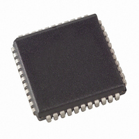
AT89LP6440-20JU Atmel, AT89LP6440-20JU Datasheet - Page 50

AT89LP6440-20JU
Manufacturer Part Number
AT89LP6440-20JU
Description
MCU 8051 64K FLASH ISP 44PLCC
Manufacturer
Atmel
Series
89LPr
Datasheet
1.AT89LP6440-20MU.pdf
(194 pages)
Specifications of AT89LP6440-20JU
Core Processor
8051
Core Size
8-Bit
Speed
20MHz
Connectivity
I²C, SPI, UART/USART
Peripherals
Brown-out Detect/Reset, POR, PWM, WDT
Number Of I /o
38
Program Memory Size
64KB (64K x 8)
Program Memory Type
FLASH
Eeprom Size
8K x 8
Ram Size
4.25K x 8
Voltage - Supply (vcc/vdd)
2.4 V ~ 3.6 V
Data Converters
A/D 8x10b
Oscillator Type
Internal
Operating Temperature
-40°C ~ 85°C
Package / Case
44-PLCC
Processor Series
AT89x
Core
8051
Data Bus Width
8 bit
Data Ram Size
8 KB
Interface Type
2-Wire, SPI
Maximum Clock Frequency
24 MHz
Number Of Programmable I/os
38
Number Of Timers
3
Operating Supply Voltage
2.7 V to 3.6 V
Maximum Operating Temperature
+ 85 C
Mounting Style
SMD/SMT
3rd Party Development Tools
PK51, CA51, A51, ULINK2
Development Tools By Supplier
AT89ISP
Minimum Operating Temperature
- 40 C
On-chip Adc
10 bit, 8 Channel
On-chip Dac
10 bit, 8 Channel
Lead Free Status / RoHS Status
Lead free / RoHS Compliant
Available stocks
Company
Part Number
Manufacturer
Quantity
Price
Company:
Part Number:
AT89LP6440-20JU
Manufacturer:
Atmel
Quantity:
103
11. Enhanced Timer 0 and Timer 1 with PWM
50
AT89LP6440 - Preliminary
The AT89LP6440 has two 16-bit Timer/Counters, Timer 0 and Timer 1, with the following
features:
Timer 0 and Timer 1 have similar modes of operation. As timers, the timer registers increase
every clock cycle by default. Thus, the registers count clock cycles. Since a clock cycle consists
of one oscillator period, the count rate is equal to the oscillator frequency. The timer rate can be
prescaled by a value between 1 and 16 using the Timer Prescaler (see
Both Timers share the same prescaler.
As counters, the timer registers are incremented in response to a 1-to-0 transition at the corre-
sponding input pins, T0 or T1. The external input is sampled every clock cycle. When the
samples show a high in one cycle and a low in the next cycle, the count is incremented. The new
count value appears in the register during the cycle following the one in which the transition was
detected. Since 2 clock cycles are required to recognize a 1-to-0 transition, the maximum count
rate is 1/2 of the oscillator frequency. There are no restrictions on the duty cycle of the input sig-
nal, but it should be held for at least one full clock cycle to ensure that a given level is sampled at
least once before it changes.
Furthermore, the Timer or Counter functions for Timer 0 and Timer 1 have four operating modes:
variable width timer, 16-bit auto-reload timer, 8-bit auto-reload timer, and split timer. The control
bits C/T in the Special Function Register TMOD select the Timer or Counter function. The bit
pairs (M1, M0) in TMOD select the operating modes.
Table 11-1.
Name
TCON
TMOD
TL0
TL1
TH0
TH1
TCONB
RL0
RL1
RH0
RH1
• Two 16-bit timer/counters with 16-bit reload registers
• Two independent 8-bit precision PWM outputs with 8-bit prescalers
• UART or SPI baud rate generation using Timer 1
• Output pin toggle on timer overflow
• Split timer mode allows for three separate timers (2 8-bit, 1 16-bit)
• Gated modes allow timers to run/halt based on an external input
Address
Timer 0/1 Register Summary
8AH
8BH
8CH
8DH
88H
89H
91H
92H
93H
94H
95H
Purpose
Control
Mode
Timer 0 low-byte
Timer 1 low-byte
Timer 0 high-byte
Timer 1 high-byte
Mode
Timer 0 reload low-byte
Timer 1 reload low-byte
Timer 0 reload high-byte
Timer 1 reload high-byte
Table 6-2 on page
Bit-Addressable
3706A–MICRO–9/09
N
N
N
N
N
N
N
N
N
N
Y
32).


