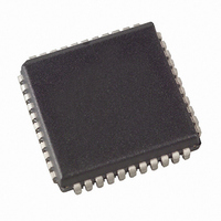
AT89LP6440-20JU Atmel, AT89LP6440-20JU Datasheet - Page 88

AT89LP6440-20JU
Manufacturer Part Number
AT89LP6440-20JU
Description
MCU 8051 64K FLASH ISP 44PLCC
Manufacturer
Atmel
Series
89LPr
Datasheet
1.AT89LP6440-20MU.pdf
(194 pages)
Specifications of AT89LP6440-20JU
Core Processor
8051
Core Size
8-Bit
Speed
20MHz
Connectivity
I²C, SPI, UART/USART
Peripherals
Brown-out Detect/Reset, POR, PWM, WDT
Number Of I /o
38
Program Memory Size
64KB (64K x 8)
Program Memory Type
FLASH
Eeprom Size
8K x 8
Ram Size
4.25K x 8
Voltage - Supply (vcc/vdd)
2.4 V ~ 3.6 V
Data Converters
A/D 8x10b
Oscillator Type
Internal
Operating Temperature
-40°C ~ 85°C
Package / Case
44-PLCC
Processor Series
AT89x
Core
8051
Data Bus Width
8 bit
Data Ram Size
8 KB
Interface Type
2-Wire, SPI
Maximum Clock Frequency
24 MHz
Number Of Programmable I/os
38
Number Of Timers
3
Operating Supply Voltage
2.7 V to 3.6 V
Maximum Operating Temperature
+ 85 C
Mounting Style
SMD/SMT
3rd Party Development Tools
PK51, CA51, A51, ULINK2
Development Tools By Supplier
AT89ISP
Minimum Operating Temperature
- 40 C
On-chip Adc
10 bit, 8 Channel
On-chip Dac
10 bit, 8 Channel
Lead Free Status / RoHS Status
Lead free / RoHS Compliant
Available stocks
Company
Part Number
Manufacturer
Quantity
Price
Company:
Part Number:
AT89LP6440-20JU
Manufacturer:
Atmel
Quantity:
103
16.3
88
More About Mode 0
AT89LP6440 - Preliminary
In Mode 0, the UART is configured as a two wire half-duplex synchronous serial interface. Serial
data enters and exits through RXD. TXD outputs the shift clock. Eight data bits are transmit-
ted/received, with the LSB first.
the serial port in Mode 0 and associated timing. The baud rate is programmable to 1/2 or 1/4 the
oscillator frequency by setting/clearing the SMOD1 bit. However, changing SMOD1 has an
effect on the relationship between the clock and data as described below. The baud rate can
also be generated by Timer 1 by setting TB8.
Table 16-4.
Transmission is initiated by any instruction that uses SBUF as a destination register. The “write
to SBUF” signal also loads a “1” into the 9th position of the transmit shift register and tells the TX
Control Block to begin a transmission. The internal timing is such that one full bit slot may elapse
between “write to SBUF” and activation of SEND.
SEND transfers the output of the shift register to the alternate output function line of P3.0, and
also transfers Shift Clock to the alternate output function line of P3.1. As data bits shift out to the
right, “0”s come in from the left. When the MSB of the data byte is at the output position of the
shift register, the “1” that was initially loaded into the 9th position is just to the left of the MSB,
and all positions to the left of that contain “0”s. This condition flags the TX Control block to do
one last shift, then deactivate SEND and set TI.
Reception is initiated by the condition REN = 1 and R1 = 0. At the next clock cycle, the RX Con-
trol unit writes the bits 11111110 to the receive shift register and activates RECEIVE in the next
clock phase. RECEIVE enables Shift Clock to the alternate output function line of P3.1. As data
bits come in from the right, “1”s shift out to the left. When the “0” that was initially loaded into the
right-most position arrives at the left-most position in the shift register, it flags the RX Control
block to do one last shift and load SBUF. Then RECEIVE is cleared and RI is set.
The relationship between the shift clock and data is determined by the combination of the SM2
and SMOD1 bits as listed in
idle state of the clock when not currently transmitting/receiving. The SMOD1 bit determines if the
output data is stable for both edges of the clock, or just one.
Table 16-5.
SM2
TB8
0
0
1
1
0
0
1
1
SMOD1
SMOD1
Mode 0 Baud Rates
0
1
0
1
Mode 0 Clock and Data Modes
0
1
0
1
Clock Idle
(Timer 1 Overflow) / 4
(Timer 1 Overflow) / 2
High
High
Low
Low
Table 16-5
Baud Rate
Figure 16-1 on page 89
f
f
SYS
SYS
/4
/2
and shown in
Negative edge of clock
Negative edge of clock
While clock is high
While clock is low
Table 16-4
Data Changed
Figure
shows a simplified functional diagram of
lists the baud rate options for Mode 0.
16-2. The SM2 bit determines the
Negative edge of clock
Positive edge of clock
Positive edge of clock
Positive edge of clock
Data Sampled
3706A–MICRO–9/09


