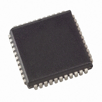
AT89LP6440-20JU Atmel, AT89LP6440-20JU Datasheet - Page 128

AT89LP6440-20JU
Manufacturer Part Number
AT89LP6440-20JU
Description
MCU 8051 64K FLASH ISP 44PLCC
Manufacturer
Atmel
Series
89LPr
Datasheet
1.AT89LP6440-20MU.pdf
(194 pages)
Specifications of AT89LP6440-20JU
Core Processor
8051
Core Size
8-Bit
Speed
20MHz
Connectivity
I²C, SPI, UART/USART
Peripherals
Brown-out Detect/Reset, POR, PWM, WDT
Number Of I /o
38
Program Memory Size
64KB (64K x 8)
Program Memory Type
FLASH
Eeprom Size
8K x 8
Ram Size
4.25K x 8
Voltage - Supply (vcc/vdd)
2.4 V ~ 3.6 V
Data Converters
A/D 8x10b
Oscillator Type
Internal
Operating Temperature
-40°C ~ 85°C
Package / Case
44-PLCC
Processor Series
AT89x
Core
8051
Data Bus Width
8 bit
Data Ram Size
8 KB
Interface Type
2-Wire, SPI
Maximum Clock Frequency
24 MHz
Number Of Programmable I/os
38
Number Of Timers
3
Operating Supply Voltage
2.7 V to 3.6 V
Maximum Operating Temperature
+ 85 C
Mounting Style
SMD/SMT
3rd Party Development Tools
PK51, CA51, A51, ULINK2
Development Tools By Supplier
AT89ISP
Minimum Operating Temperature
- 40 C
On-chip Adc
10 bit, 8 Channel
On-chip Dac
10 bit, 8 Channel
Lead Free Status / RoHS Status
Lead free / RoHS Compliant
Available stocks
Company
Part Number
Manufacturer
Quantity
Price
Company:
Part Number:
AT89LP6440-20JU
Manufacturer:
Atmel
Quantity:
103
19.2
19.3
128
Internal Reference Voltage
Comparator Interrupt Debouncing
AT89LP6440 - Preliminary
Figure 19-2. Equivalent Analog Input Model
The negative input terminal of each comparator may be connected to an internal voltage refer-
ence by changing the RFB
set to 1.25 V ±5%. The voltage reference also provides two additional voltage levels approxi-
mately 125 mV above and below V
as an internally referenced window comparator with up to four input channels. Changing the ref-
erence input must follow the same routine used for changing the positive input as described in
“Analog Input Muxes”
The comparator output is normally sampled every clock cycle. The conditions on the analog
inputs may be such that the comparator output will toggle excessively. This is especially true if
applying slow moving analog inputs. Three debouncing modes are provided to filter out this
noise for edge-triggered interrupts. In debouncing mode, the comparator uses Timer 1 to modu-
late its sampling time when CxC
waits until two Timer 1 overflows have occurred before resampling the output. If the new sample
agrees with the expected value, CFx is set. Otherwise, the event is ignored. The filter may be
tuned by adjusting the time-out period of Timer 1. Because Timer 1 is free running, the
debouncer must wait for two overflows to guarantee that the sampling delay is at least 1 time-out
period. Therefore, after the initial edge event, the interrupt may occur between 1 and 2 time-out
periods later. See
flows, i.e. CxC
be accepted as an edge event.
Figure 19-3. Negative Edge with Debouncing Example
Timer 1 Overflow
Comparator Out
AINn
1-0
!= 00B, any change in the comparator output must be valid after 4 samples to
Figure
CFx
C
10 pF
PIN
above.
Start
19-3. When the comparator clock is provided by one of the timer over-
=
1-0
or RFA
1-0
AREF
= 00B. When a relevant transition occurs, the comparator
1-0
. These levels may be used to configure the comparators
bits in AREF. The internal reference voltage, V
(rejected)
Compare
10 kΩ
R
IN
=
Start
R
10 kΩ
MUX
=
(accepted)
Compare
C
0.3 pF
CMP
<
3706A–MICRO–9/09
AREF
, is


