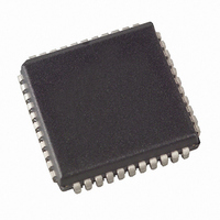
AT89LP6440-20JU Atmel, AT89LP6440-20JU Datasheet - Page 157

AT89LP6440-20JU
Manufacturer Part Number
AT89LP6440-20JU
Description
MCU 8051 64K FLASH ISP 44PLCC
Manufacturer
Atmel
Series
89LPr
Datasheet
1.AT89LP6440-20MU.pdf
(194 pages)
Specifications of AT89LP6440-20JU
Core Processor
8051
Core Size
8-Bit
Speed
20MHz
Connectivity
I²C, SPI, UART/USART
Peripherals
Brown-out Detect/Reset, POR, PWM, WDT
Number Of I /o
38
Program Memory Size
64KB (64K x 8)
Program Memory Type
FLASH
Eeprom Size
8K x 8
Ram Size
4.25K x 8
Voltage - Supply (vcc/vdd)
2.4 V ~ 3.6 V
Data Converters
A/D 8x10b
Oscillator Type
Internal
Operating Temperature
-40°C ~ 85°C
Package / Case
44-PLCC
Processor Series
AT89x
Core
8051
Data Bus Width
8 bit
Data Ram Size
8 KB
Interface Type
2-Wire, SPI
Maximum Clock Frequency
24 MHz
Number Of Programmable I/os
38
Number Of Timers
3
Operating Supply Voltage
2.7 V to 3.6 V
Maximum Operating Temperature
+ 85 C
Mounting Style
SMD/SMT
3rd Party Development Tools
PK51, CA51, A51, ULINK2
Development Tools By Supplier
AT89ISP
Minimum Operating Temperature
- 40 C
On-chip Adc
10 bit, 8 Channel
On-chip Dac
10 bit, 8 Channel
Lead Free Status / RoHS Status
Lead free / RoHS Compliant
Available stocks
Company
Part Number
Manufacturer
Quantity
Price
Company:
Part Number:
AT89LP6440-20JU
Manufacturer:
Atmel
Quantity:
103
25. Programming the Flash Memory
25.1
3706A–MICRO–9/09
Physical Interface
The Atmel AT89LP6440 microcontroller features 64K bytes of on-chip In-System Programmable
Flash program memory and 8K bytes of nonvolatile Flash data memory. In-System Program-
ming allows programming and reprogramming of the microcontroller positioned inside the end
system. Using a simple 4-wire SPI interface, the programmer communicates serially with the
AT89LP6440 microcontroller, reprogramming all nonvolatile memories on the chip. In-System
Programming eliminates the need for physical removal of the chips from the system. This will
save time and money, both during development in the lab, and when updating the software or
parameters in the field. The programming interface of the AT89LP6440 includes the following
features:
For more detailed information on In-System Programming, refer to the Application Note entitled
“AT89LP In-System Programming Specification”.
The AT89LP6440 provides a standard programming command set with two physical interfaces:
a bit-serial and a byte-parallel interface. Normal Flash programming utilizes the Serial Peripheral
Interface (SPI) pins of an AT89LP6440 microcontroller. The SPI is a full-duplex synchronous
serial interface consisting of four wires: Serial Clock (SCK), Master-In/Slave-out (MISO), Master-
out/Slave-in (MOSI), and an active-low Slave Select (SS). When programming an AT89LP6440
device, the programmer always operates as the SPI master, and the target system always oper-
ates as the SPI slave. To enter or remain in Programming mode the device’s reset line (RST)
must be held active (low). With the addition of VDD and GND, an AT89LP6440 microcontroller
can be programmed with a minimum of seven connections as shown in
• When using the Internal RC Oscillator during debug, DDA is located on the XTAL1/P4.0 pin.
• When using the External Clock during debug, DDA is located on the XTAL2/P4.1 pin and the
• When using the Crystal Oscillator during debug, DDA is located on the P4.3 pin and the
• Four-wire serial SPI Programming Interface or 11-pin Parallel Interface
• Active-low Reset Entry into Programming
• Slave Select allows multiple devices on same interface
• User Signature Array
• Flexible Page Programming
• Row Erase Capability
• Page Write with Auto-Erase Commands
• Programming Status Register
The P4.0 I/O function cannot be emulated in this mode.
system clock drives XTAL1/P4.0. The P4.1 I/O and CLKOUT functions cannot be emulated in
this mode.
crystal connects to XTAL1/P4.0 and XTAL2/P4.1. The P4.3 I/O function cannot be emulated
in this mode.
AT89LP6440 - Preliminary
Figure
25-1.
157


